ATAVRSB100 Atmel, ATAVRSB100 Datasheet - Page 15
ATAVRSB100
Manufacturer Part Number
ATAVRSB100
Description
SMART BATTERY DEVELOPMENT KIT
Manufacturer
Atmel
Type
Smart Batteryr
Datasheet
1.ATAVRSB100.pdf
(20 pages)
Specifications of ATAVRSB100
Contents
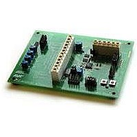
Fully Assembled Evaluation Board
Processor
ATmega406
Processor To Be Evaluated
ATmega406
Data Bus Width
8 bit
Interface Type
JTAG
For Use With/related Products
ATmega406
Lead Free Status / RoHS Status
Contains lead / RoHS non-compliant
Other names
Q2367281


2598C-AVR-06/06
Thus, it is better to use lower resistance thermistors to reduce errors. Figure 2-7
shows how to connect external thermistors to HDR1.
Since the input impedance of the VADC will affect the reading, PA0 is used both for
normal readings and to provide a ‘calibration’ reading. Specifically, PA0 is selected as
a VADC input and a conversion is performed, while PA1-4 are configured as digital
inputs without pull-up resistors enabled. Since the PA0 pin provides an impedance to
GND, the voltage on the PA0 pin, and the thermistor common bus, will not be 1.100V,
but will reflect the voltage divider that is created by R25 and the VADC input
impedance. The conversion result can be used to calculate the exact input
impedance of the VADC, since R25 is a known fixed resistance. Any thermal
influence or device-to-device variance of the input impedance can also be
determined.
To read any of the four thermistors, its I/O line is driven low, thus forming a voltage
divider between R25 and the selected thermistor. A VADC conversion may optionally
be performed on that I/O signal to determine any offset above GND that may exist. A
conversion is also performed on PA0, thus reading the bus voltage. Since R25 is a
known value, the thermistor’s resistance may now be calculated, remembering that
the input impedance of the VADC itself is in parallel with the thermistor.
It is possible to have more than four external thermistors, since each thermistor
simply requires being driven low when enabled and being high impedance when not
enabled.
Table 2-10. HDR1: Thermistor connections
Figure 2-7. External thermistor connection
Pin
1
2
3
4
5
6
7
8
9
10
VREF
R25
Internal wiring
Name
ThermBUS
PA0
ThermBUS
PA1
ThermBUS
PA2
ThermBUS
PA3
ThermBUS
PA4
1
3
5
7
9
HDR1
External wiring
10
2
4
6
8
Direction
Input
Usage
Thermistor VADC input
Thermistor #1 control signal
Thermistor #2 control signal
Thermistor #3 control signal
Thermistor #4 control signal
AVR454
15
Related parts for ATAVRSB100
Image
Part Number
Description
Manufacturer
Datasheet
Request
R

Part Number:
Description:
DEV KIT FOR AVR/AVR32
Manufacturer:
Atmel
Datasheet:

Part Number:
Description:
INTERVAL AND WIPE/WASH WIPER CONTROL IC WITH DELAY
Manufacturer:
ATMEL Corporation
Datasheet:
Part Number:
Description:
Low-Voltage Voice-Switched IC for Hands-Free Operation
Manufacturer:
ATMEL Corporation
Datasheet:
Part Number:
Description:
MONOLITHIC INTEGRATED FEATUREPHONE CIRCUIT
Manufacturer:
ATMEL Corporation
Datasheet:
Part Number:
Description:
AM-FM Receiver IC U4255BM-M
Manufacturer:
ATMEL Corporation
Datasheet:
Part Number:
Description:
Monolithic Integrated Feature Phone Circuit
Manufacturer:
ATMEL Corporation
Datasheet:
Part Number:
Description:
Multistandard Video-IF and Quasi Parallel Sound Processing
Manufacturer:
ATMEL Corporation
Datasheet:
Part Number:
Description:
High-performance EE PLD
Manufacturer:
ATMEL Corporation
Datasheet:
Part Number:
Description:
8-bit Flash Microcontroller
Manufacturer:
ATMEL Corporation
Datasheet:
Part Number:
Description:
2-Wire Serial EEPROM
Manufacturer:
ATMEL Corporation
Datasheet: