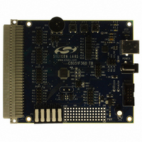
C8051F360-TB Silicon Laboratories Inc, C8051F360-TB Datasheet - Page 174

C8051F360-TB
Manufacturer Part Number
C8051F360-TB
Description
BOARD TARGET/PROTO W/C8051F360
Manufacturer
Silicon Laboratories Inc
Type
MCUr
Specifications of C8051F360-TB
Contents
Board
Processor To Be Evaluated
C8051F36x
Interface Type
USB
Lead Free Status / RoHS Status
Lead free / RoHS Compliant
For Use With/related Products
C8051F360
Lead Free Status / Rohs Status
Lead free / RoHS Compliant
Other names
336-1412
- Current page: 174 of 288
- Download datasheet (3Mb)
C8051F360/1/2/3/4/5/6/7/8/9
174
Bits 7–6: RESERVED. Read = 00b. Must Write 00b.
Bits 5–4: CLKDIV1-0: Output SYSCLK Divide Factor.
Bit 3:
Bits 2–0: CLKSL2–0: System Clock Source Select Bits.
SFR Page:
SFR Address:
Reserved Reserved CLKDIV1 CLKDIV0 Reserved CLKSL2
R/W
Bit7
These bits can be used to pre-divide SYSCLK before it is output to a port pin through the
crossbar.
00: Output will be SYSCLK.
01: Output will be SYSCLK/2.
10: Output will be SYSCLK/4.
11: Output will be SYSCLK/8.
See Section “17. Port Input/Output” on page 183 for more details about routing this output to
a port pin.
RESERVED. Read = 0b. Must Write 0b.
000: SYSCLK derived from the high-frequency Internal Oscillator, and scaled as per the
001: SYSCLK derived from the External Oscillator circuit.
010: SYSCLK derived from the low-frequency Internal Oscillator, and scaled as per the
011: RESERVED.
100: SYSCLK derived from the PLL.
101-11x: RESERVED.
F
0x8F
IFCN bits in OSCICN.
OSCLD bits in OSCLCN.
R/W
Bit6
SFR Definition 16.4. CLKSEL: System Clock Selection
R/W
Bit5
R/W
Bit4
Rev. 1.0
R/W
Bit3
R/W
Bit2
CLKSL1
R/W
Bit1
CLKSL0 00000000
R/W
Bit0
Reset Value
Related parts for C8051F360-TB
Image
Part Number
Description
Manufacturer
Datasheet
Request
R
Part Number:
Description:
SMD/C°/SINGLE-ENDED OUTPUT SILICON OSCILLATOR
Manufacturer:
Silicon Laboratories Inc
Part Number:
Description:
Manufacturer:
Silicon Laboratories Inc
Datasheet:
Part Number:
Description:
N/A N/A/SI4010 AES KEYFOB DEMO WITH LCD RX
Manufacturer:
Silicon Laboratories Inc
Datasheet:
Part Number:
Description:
N/A N/A/SI4010 SIMPLIFIED KEY FOB DEMO WITH LED RX
Manufacturer:
Silicon Laboratories Inc
Datasheet:
Part Number:
Description:
N/A/-40 TO 85 OC/EZLINK MODULE; F930/4432 HIGH BAND (REV E/B1)
Manufacturer:
Silicon Laboratories Inc
Part Number:
Description:
EZLink Module; F930/4432 Low Band (rev e/B1)
Manufacturer:
Silicon Laboratories Inc
Part Number:
Description:
I°/4460 10 DBM RADIO TEST CARD 434 MHZ
Manufacturer:
Silicon Laboratories Inc
Part Number:
Description:
I°/4461 14 DBM RADIO TEST CARD 868 MHZ
Manufacturer:
Silicon Laboratories Inc
Part Number:
Description:
I°/4463 20 DBM RFSWITCH RADIO TEST CARD 460 MHZ
Manufacturer:
Silicon Laboratories Inc
Part Number:
Description:
I°/4463 20 DBM RADIO TEST CARD 868 MHZ
Manufacturer:
Silicon Laboratories Inc
Part Number:
Description:
I°/4463 27 DBM RADIO TEST CARD 868 MHZ
Manufacturer:
Silicon Laboratories Inc
Part Number:
Description:
I°/4463 SKYWORKS 30 DBM RADIO TEST CARD 915 MHZ
Manufacturer:
Silicon Laboratories Inc
Part Number:
Description:
N/A N/A/-40 TO 85 OC/4463 RFMD 30 DBM RADIO TEST CARD 915 MHZ
Manufacturer:
Silicon Laboratories Inc
Part Number:
Description:
I°/4463 20 DBM RADIO TEST CARD 169 MHZ
Manufacturer:
Silicon Laboratories Inc


