AT91SAM7A1-EK Atmel, AT91SAM7A1-EK Datasheet - Page 16
AT91SAM7A1-EK
Manufacturer Part Number
AT91SAM7A1-EK
Description
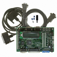
BOARD EVAL FOR AT91SAM7A1
Manufacturer
Atmel
Series
AT91SAM Smart ARMr
Type
MCUr
Datasheet
1.AT91SAM7A1-EK.pdf
(31 pages)
Specifications of AT91SAM7A1-EK
Contents
Evaluation Board, Parallel Cable and CD-ROM
Processor To Be Evaluated
AT91SAM7A1
Data Bus Width
32 bit
Interface Type
RS-232
For Use With/related Products
AT91SAM7A1
Lead Free Status / RoHS Status
Contains lead / RoHS non-compliant
Available stocks
Company
Part Number
Manufacturer
Quantity
Price
Company:

Part Number:
AT91SAM7A1-EK
Manufacturer:
Atmel
Quantity:
2


6114A–ATARM–09/04
3.9
3.10
3-6
I/O Expansion
External Bus
Interface
To protect the upper memory and access only the lower memory (from 0x40000000 to
0x40080000: only 1 Mbyte), put a jumper in J5: 2 - 3.
To protect the lower memory and access only the upper memory (from 0x40080000 to
0x40100000: only 1 Mbyte), close the jumper from J5: 2 - 3.
The mapping defined by the boot software is shown in Table 3-10.
Table 3-10. Memory Mapping
Two I/O expansion connectors (J17 and J18) provide the users with the general-pur-
pose I/O (GPIO) lines, analog lines, VDD and ground. The connectors are not fitted at
the factory; however, the user can fit any 2 x 25 connector on a 0.1" (2.54 mm) pitch. For
connector pin-out details, see Figure 4-10.
Figure 4-8 shows one 2 MByte 16-bit Flash (AT49BV1614A-90TC) and a 512 Kbyte 16-
bit SRAM device (Alliance AS7C34098-10TC or equivalent).
Figure 4-9 shows the bus expansion connector (J16) that, like the I/O expansion con-
nector (J17 and J18), is not fitted at the factory. The user can fit any 32 x 2 connector on
a 0.1" (2.54 mm) pitch to gain access to the data, address, chip select, read/write, oscil-
lator output and wait state pins. VDD and ground are available on the connector.
On-board jumpers (J13, J14 and J15) allow the user to connect Chip Selects either to
on-board memories or to the expansion connector.
In most case, jumpers should be set up as in Table 3-11.
Table 3-11. Board Jumper Configuration
Jumper
J13
J14
J15
Element
SRAM
Flash
Jumper Configuration
1 - 2 left open
1 - 2 left open
2 - 3 left open
1 - 2 left open
1 - 2 left open
2 - 3 left open
1 - 2 closed
1 - 2 closed
1 - 2 closed
2 - 3 closed
AT91SAM7A1-EK Evaluation Board User Guide
protected. User can access only the 1
protected. User can access only the 1
On-board SRAM always de-selected
On-board Flash always de-selected
driven. User can access the whole
On-board Flash address line 20 is
On-board SRAM driven by NCS1
On-board Flash driven by NCS0
On-board Flash upper memory
On-board Flash lower memory
Mbyte upper space.
0x40000000
0x48000000
Mbyte lower space.
Address
memory space.
Description
Related parts for AT91SAM7A1-EK
Image
Part Number
Description
Manufacturer
Datasheet
Request
R

Part Number:
Description:
MCU ARM9 64K SRAM 144-LFBGA
Manufacturer:
Atmel
Datasheet:

Part Number:
Description:
IC ARM7 MCU FLASH 256K 100LQFP
Manufacturer:
Atmel
Datasheet:

Part Number:
Description:
IC ARM9 MPU 217-LFBGA
Manufacturer:
Atmel
Datasheet:
Part Number:
Description:
MCU ARM9 ULTRA LOW PWR 217-LFBGA
Manufacturer:
Atmel
Datasheet:

Part Number:
Description:
MCU ARM9 324-TFBGA
Manufacturer:
Atmel
Datasheet:
Part Number:
Description:
IC MCU ARM9 SAMPLING 217CBGA
Manufacturer:
Atmel
Datasheet:
Part Number:
Description:
IC ARM9 MCU 217-LFBGA
Manufacturer:
Atmel
Datasheet:

Part Number:
Description:
IC ARM9 MCU 208-PQFP
Manufacturer:
Atmel
Datasheet:
Part Number:
Description:
MCU ARM 512K HS FLASH 100-LQFP
Manufacturer:
Atmel
Datasheet:

Part Number:
Description:
MCU ARM 512K HS FLASH 100-TFBGA
Manufacturer:
Atmel
Datasheet:
Part Number:
Description:
IC ARM9 MCU 200 MHZ 324-TFBGA
Manufacturer:
Atmel
Datasheet:

Part Number:
Description:
IC ARM MCU 16BIT 128K 256BGA
Manufacturer:
Atmel
Datasheet:

Part Number:
Description:
IC ARM7 MCU 32BIT 128K 64LQFP
Manufacturer:
Atmel
Datasheet:

Part Number:
Description:
IC ARM7 MCU FLASH 256K 128-LQFP
Manufacturer:
Atmel
Datasheet:
Part Number:
Description:
IC ARM7 MCU FLASH 512K 128-LQFP
Manufacturer:
Atmel
Datasheet: