HW-V5-ML501-UNI-G Xilinx Inc, HW-V5-ML501-UNI-G Datasheet - Page 36
HW-V5-ML501-UNI-G
Manufacturer Part Number
HW-V5-ML501-UNI-G
Description
EVALUATION PLATFORM VIRTEX-5
Manufacturer
Xilinx Inc
Series
Virtex™-5 LXr
Type
FPGAr
Datasheet
1.HW-V5-ML501-UNI-G.pdf
(42 pages)
Specifications of HW-V5-ML501-UNI-G
Design Resources
ML501 Ref Design User Guide ML501 Schematics
Contents
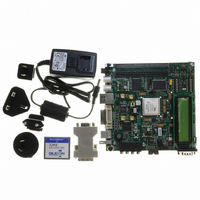
ML501 Platform, DVI Adapter and CompactFlash Card
Silicon Manufacturer
Xilinx
Features
Programmable System Clock Generator Chip, RS-232 Serial Port
Silicon Family Name
Virtex-5
Silicon Core Number
XC5VLX50FFG676
Lead Free Status / RoHS Status
Lead free / RoHS Compliant
For Use With/related Products
XC5VLX50FFG676
Lead Free Status / RoHS Status
Lead free / RoHS Compliant, Lead free / RoHS Compliant
Other names
122-1508
Available stocks
Company
Part Number
Manufacturer
Quantity
Price


Chapter 1: ML501 Evaluation Platform
Configuration Options
36
JTAG (Xilinx Download Cable and System ACE Controller) Configuration
The FPGA on the ML501 Evaluation Platform can be configured by five major devices:
•
•
•
•
•
The following section provides an overview of the possible ways the FPGA can be
configured.
The FPGA, Platform Flash PROM, and CPLD can be configured through the JTAG port.
The JTAG chain of the board is illustrated in
The chain starts at the PC4 connector and goes through the System ACE controller, the
Platform Flash PROM, the FPGA, the CPLD, and an optional extension of the chain to the
expansion card. Jumper J21 determines if the JTAG chain should be extended to the
expansion card.
The JTAG chain can be used to program the FPGA and access the FPGA for hardware and
software debug. The JTAG chain is also used to program the Platform Flash PROM and the
CPLD.
The PC4 JTAG connection to the JTAG chain allows a host computer to download
bitstreams to the FPGA using the iMPACT software tool. PC4 also allows debug tools such
as the ChipScope™ Pro Analyzer or a software debugger to access the FPGA.
The System ACE controller can also program the FPGA through the JTAG port. Using an
inserted CompactFlash card, configuration information can be stored and played out to
the FPGA. The System ACE controller supports up to eight configuration images that can
selected using the three configuration address DIP switches. Under FPGA control, the
System ACE chip can be instructed to reconfigure to any of the eight configuration images.
The configuration mode should be set to 101. Jumper J21 should exclude the expansion
card from the JTAG chain, and switch SW15, pin 8 should be ON to use System ACE
configuration. When set correctly, the System ACE controller programs the FPGA upon
power-up if a CompactFlash card is present or whenever a CompactFlash card is inserted.
Pressing the System ACE reset button also causes the System ACE controller to program
the FPGA if a CompactFlash card is present.
Xilinx download cable (JTAG)
System ACE controller (JTAG)
Platform Flash PROM
Linear Flash memory
SPI Flash memory
J1
Platform Flash
Memory
TDI
TDO
www.xilinx.com
TDI
CPLD
TDO
Figure 1-5: JTAG Chain
TSTTDI
TSTDO
System ACE
Controller
Figure
CFGTDO
CFGTDI
1-5.
TDI
UG226 (v1.4) August 24, 2009
J21
FPGA
1
2
3
ML501 Evaluation Platform
TDO
Expansion
TDI
TDO
UG226_05_082906
R
Related parts for HW-V5-ML501-UNI-G
Image
Part Number
Description
Manufacturer
Datasheet
Request
R

Part Number:
Description:
IC CPLD .8K 36MCELL 44-VQFP
Manufacturer:
Xilinx Inc
Datasheet:

Part Number:
Description:
IC CPLD 72MCRCELL 10NS 44VQFP
Manufacturer:
Xilinx Inc
Datasheet:

Part Number:
Description:
IC CPLD 1.6K 72MCELL 64-VQFP
Manufacturer:
Xilinx Inc
Datasheet:

Part Number:
Description:
IC CR-II CPLD 64MCELL 44-VQFP
Manufacturer:
Xilinx Inc
Datasheet:

Part Number:
Description:
IC CPLD 1.6K 72MCELL 100-TQFP
Manufacturer:
Xilinx Inc
Datasheet:

Part Number:
Description:
IC CR-II CPLD 64MCELL 56-BGA
Manufacturer:
Xilinx Inc
Datasheet:

Part Number:
Description:
IC CPLD 72MCRCELL 7.5NS 44VQFP
Manufacturer:
Xilinx Inc
Datasheet:
Part Number:
Description:
IC CR-II CPLD 64MCELL 100-VQFP
Manufacturer:
Xilinx Inc
Datasheet:
Part Number:
Description:
IC CPLD 1.6K 72MCELL 100-TQFP
Manufacturer:
Xilinx Inc
Datasheet:

Part Number:
Description:
IC CPLD 72MCRCELL 7.5NS 64VQFP
Manufacturer:
Xilinx Inc
Datasheet:
Part Number:
Description:
IC CPLD 1.6K 72MCELL 100-TQFP
Manufacturer:
Xilinx Inc
Datasheet:

Part Number:
Description:
IC CPLD 1.5K 64MCELL HP 44-VQFP
Manufacturer:
Xilinx Inc

Part Number:
Description:
IC CPLD 36MCRCELL 15NS 44PLCC
Manufacturer:
Xilinx Inc
Datasheet:

Part Number:
Description:
IC CPLD 36MCRCELL 10NS 44PLCC
Manufacturer:
Xilinx Inc
Datasheet:

Part Number:
Description:
IC CPLD 1.5K 64MCELL HP 44-VQFP
Manufacturer:
Xilinx Inc