HW-V5-ML501-UNI-G Xilinx Inc, HW-V5-ML501-UNI-G Datasheet - Page 20
HW-V5-ML501-UNI-G
Manufacturer Part Number
HW-V5-ML501-UNI-G
Description
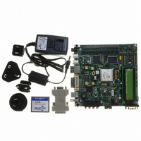
EVALUATION PLATFORM VIRTEX-5
Manufacturer
Xilinx Inc
Series
Virtex™-5 LXr
Type
FPGAr
Datasheet
1.HW-V5-ML501-UNI-G.pdf
(42 pages)
Specifications of HW-V5-ML501-UNI-G
Design Resources
ML501 Ref Design User Guide ML501 Schematics
Contents
ML501 Platform, DVI Adapter and CompactFlash Card
Silicon Manufacturer
Xilinx
Features
Programmable System Clock Generator Chip, RS-232 Serial Port
Silicon Family Name
Virtex-5
Silicon Core Number
XC5VLX50FFG676
Lead Free Status / RoHS Status
Lead free / RoHS Compliant
For Use With/related Products
XC5VLX50FFG676
Lead Free Status / RoHS Status
Lead free / RoHS Compliant, Lead free / RoHS Compliant
Other names
122-1508
Available stocks
Company
Part Number
Manufacturer
Quantity
Price


Chapter 1: ML501 Evaluation Platform
20
8. User Pushbuttons (Active-High)
9. CPU Reset Button (Active-Low)
10. XGI Expansion Headers
Differential Expansion I/O Connectors
Five active-High user pushbuttons are available for general purpose usage and are
arranged in a North-East-South-West-Center orientation (only the center one is cited in
Figure 1-2, page
Table 1-7: User Pushbutton Connections
The CPU reset button is an active-Low pushbutton and is used as a system or user reset
button. This pushbutton switch is wired only to an FPGA I/O pin so it can also be used as
a general-purpose pushbutton switch (see
Table 1-8: CPU Reset Connections
The board contains expansion headers for easy expansion or adaptation of the board for
other applications. The expansion connectors use standard 0.1-inch headers. The
expansion connectors contain connections to single-ended and differential FPGA I/Os,
ground, 2.5V/3.3V/5V power, JTAG chain, and the IIC bus. All signals on connectors J4
and J6 have matched length traces that are matched to each other.
Header J4 contains 16 pairs of differential signal connections to the FPGA I/Os. This
permits the signals on this connector to carry high-speed differential signals, such as LVDS
data. All differential signals are routed with 100Ω differential trace impedance. Matched
length traces are used across all differential signals on J4. Consequently, these signals
connect to the FPGA I/O, and they can be used as independent single-ended nets. The
V
summarizes the differential connections on this expansion I/O connector.
CCIO
Designator
Designator
Reference
Reference
SW10
SW12
SW13
SW14
SW11
SW3
of these signals can be set to 2.5V or 3.3V by setting jumper J20.
12).
N (GPIO North)
E (GPIO East)
S (GPIO South)
W (GPIO West)
C (GPIO Center)
Table 1-7
Label/Definition
Label/Definition
CPU RESET
www.xilinx.com
summarizes the user pushbutton connections.
Table
FPGA Pin
FPGA Pin
1-8).
A22
A23
C21
T23
B22
B21
UG226 (v1.4) August 24, 2009
ML501 Evaluation Platform
Table 1-9, page 21
R
Related parts for HW-V5-ML501-UNI-G
Image
Part Number
Description
Manufacturer
Datasheet
Request
R

Part Number:
Description:
IC CPLD .8K 36MCELL 44-VQFP
Manufacturer:
Xilinx Inc
Datasheet:

Part Number:
Description:
IC CPLD 72MCRCELL 10NS 44VQFP
Manufacturer:
Xilinx Inc
Datasheet:

Part Number:
Description:
IC CPLD 1.6K 72MCELL 64-VQFP
Manufacturer:
Xilinx Inc
Datasheet:

Part Number:
Description:
IC CR-II CPLD 64MCELL 44-VQFP
Manufacturer:
Xilinx Inc
Datasheet:

Part Number:
Description:
IC CPLD 1.6K 72MCELL 100-TQFP
Manufacturer:
Xilinx Inc
Datasheet:

Part Number:
Description:
IC CR-II CPLD 64MCELL 56-BGA
Manufacturer:
Xilinx Inc
Datasheet:

Part Number:
Description:
IC CPLD 72MCRCELL 7.5NS 44VQFP
Manufacturer:
Xilinx Inc
Datasheet:
Part Number:
Description:
IC CR-II CPLD 64MCELL 100-VQFP
Manufacturer:
Xilinx Inc
Datasheet:
Part Number:
Description:
IC CPLD 1.6K 72MCELL 100-TQFP
Manufacturer:
Xilinx Inc
Datasheet:

Part Number:
Description:
IC CPLD 72MCRCELL 7.5NS 64VQFP
Manufacturer:
Xilinx Inc
Datasheet:
Part Number:
Description:
IC CPLD 1.6K 72MCELL 100-TQFP
Manufacturer:
Xilinx Inc
Datasheet:

Part Number:
Description:
IC CPLD 1.5K 64MCELL HP 44-VQFP
Manufacturer:
Xilinx Inc

Part Number:
Description:
IC CPLD 36MCRCELL 15NS 44PLCC
Manufacturer:
Xilinx Inc
Datasheet:

Part Number:
Description:
IC CPLD 36MCRCELL 10NS 44PLCC
Manufacturer:
Xilinx Inc
Datasheet:

Part Number:
Description:
IC CPLD 1.5K 64MCELL HP 44-VQFP
Manufacturer:
Xilinx Inc