HW-V5-ML501-UNI-G Xilinx Inc, HW-V5-ML501-UNI-G Datasheet - Page 25
HW-V5-ML501-UNI-G
Manufacturer Part Number
HW-V5-ML501-UNI-G
Description
EVALUATION PLATFORM VIRTEX-5
Manufacturer
Xilinx Inc
Series
Virtex™-5 LXr
Type
FPGAr
Datasheet
1.HW-V5-ML501-UNI-G.pdf
(42 pages)
Specifications of HW-V5-ML501-UNI-G
Design Resources
ML501 Ref Design User Guide ML501 Schematics
Contents
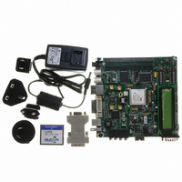
ML501 Platform, DVI Adapter and CompactFlash Card
Silicon Manufacturer
Xilinx
Features
Programmable System Clock Generator Chip, RS-232 Serial Port
Silicon Family Name
Virtex-5
Silicon Core Number
XC5VLX50FFG676
Lead Free Status / RoHS Status
Lead free / RoHS Compliant
For Use With/related Products
XC5VLX50FFG676
Lead Free Status / RoHS Status
Lead free / RoHS Compliant, Lead free / RoHS Compliant
Other names
122-1508
Available stocks
Company
Part Number
Manufacturer
Quantity
Price


ML501 Evaluation Platform
UG226 (v1.4) August 24, 2009
11. Stereo AC97 Audio Codec
12. RS-232 Serial Port
13. 16-Character x 2-Line LCD
R
The ML501 board has an AC97 audio codec (U16) to permit audio processing. The Analog
Devices AD1981 Audio Codec supports stereo 16-bit audio with up to 48-kHz sampling.
The sampling rate for record and playback can be different.
Note:
is designed to be asserted at power-on or at system reset.
Separate audio jacks are provided for Microphone, Line In, Line Out, and Headphone. All
jacks are stereo except for Microphone. The Headphone jack is driven by the audio codec's
internal 50-mW amplifier. The SPDIF jack supplies digital audio output from the codec.
Table 1-12
Table 1-12: ML501 Audio Jacks
The ML501 board contains one male DB-9 RS-232 serial port, allowing the FPGA to
communicate serial data with another device. The serial port is wired as a host (DCE)
device. Therefore, a null modem cable is normally required to connect the board to the
serial port on a computer. The serial port is designed to operate up to 115200 Bd. An
interface chip is used to shift the voltage level between FPGA and RS-232 signals.
Note:
RS-232 signals, including hardware flow-control signals, are not used. Flow control should be
disabled when communicating with a computer.
A secondary serial interface is available by using header J30 to support debug of the USB
controller chip. Header J30 brings out RS-232 voltage level signals for ground, TX data, and
RX data.
The ML501 board has a 16-character x 2-line LCD (Tianma TM162VBA6) on the board to
display text information. Potentiometer R87 adjusts the contrast of the LCD. The data
interface to the LCD is connected to the FPGA to support 4-bit mode only. The CPLD is
used to shift the voltage level between the FPGA and the LCD. The LCD module has a
connector that allows the LCD to be removed from the board to access to the components
below it.
Designator
Reference
Caution!
P10
P12
P13
P14
P11
The reset for the AC97 codec is shared with the reset signal for the flash memory chips and
The FPGA is connected only to the TX and RX data pins on the serial port. Therefore, other
summarizes the audio jacks.
Care should be taken not to scratch or damage the surface of the LCD window.
Analog Line - Out
Headphone - Out
Microphone - In
Analog Line - In
SPDIF - Out
Function
www.xilinx.com
Detailed Description
25
Related parts for HW-V5-ML501-UNI-G
Image
Part Number
Description
Manufacturer
Datasheet
Request
R

Part Number:
Description:
IC CPLD .8K 36MCELL 44-VQFP
Manufacturer:
Xilinx Inc
Datasheet:

Part Number:
Description:
IC CPLD 72MCRCELL 10NS 44VQFP
Manufacturer:
Xilinx Inc
Datasheet:

Part Number:
Description:
IC CPLD 1.6K 72MCELL 64-VQFP
Manufacturer:
Xilinx Inc
Datasheet:

Part Number:
Description:
IC CR-II CPLD 64MCELL 44-VQFP
Manufacturer:
Xilinx Inc
Datasheet:

Part Number:
Description:
IC CPLD 1.6K 72MCELL 100-TQFP
Manufacturer:
Xilinx Inc
Datasheet:

Part Number:
Description:
IC CR-II CPLD 64MCELL 56-BGA
Manufacturer:
Xilinx Inc
Datasheet:

Part Number:
Description:
IC CPLD 72MCRCELL 7.5NS 44VQFP
Manufacturer:
Xilinx Inc
Datasheet:
Part Number:
Description:
IC CR-II CPLD 64MCELL 100-VQFP
Manufacturer:
Xilinx Inc
Datasheet:
Part Number:
Description:
IC CPLD 1.6K 72MCELL 100-TQFP
Manufacturer:
Xilinx Inc
Datasheet:

Part Number:
Description:
IC CPLD 72MCRCELL 7.5NS 64VQFP
Manufacturer:
Xilinx Inc
Datasheet:
Part Number:
Description:
IC CPLD 1.6K 72MCELL 100-TQFP
Manufacturer:
Xilinx Inc
Datasheet:

Part Number:
Description:
IC CPLD 1.5K 64MCELL HP 44-VQFP
Manufacturer:
Xilinx Inc

Part Number:
Description:
IC CPLD 36MCRCELL 15NS 44PLCC
Manufacturer:
Xilinx Inc
Datasheet:

Part Number:
Description:
IC CPLD 36MCRCELL 10NS 44PLCC
Manufacturer:
Xilinx Inc
Datasheet:

Part Number:
Description:
IC CPLD 1.5K 64MCELL HP 44-VQFP
Manufacturer:
Xilinx Inc