HW-V5-ML501-UNI-G Xilinx Inc, HW-V5-ML501-UNI-G Datasheet - Page 30
HW-V5-ML501-UNI-G
Manufacturer Part Number
HW-V5-ML501-UNI-G
Description
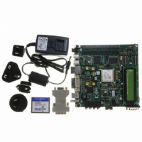
EVALUATION PLATFORM VIRTEX-5
Manufacturer
Xilinx Inc
Series
Virtex™-5 LXr
Type
FPGAr
Datasheet
1.HW-V5-ML501-UNI-G.pdf
(42 pages)
Specifications of HW-V5-ML501-UNI-G
Design Resources
ML501 Ref Design User Guide ML501 Schematics
Contents
ML501 Platform, DVI Adapter and CompactFlash Card
Silicon Manufacturer
Xilinx
Features
Programmable System Clock Generator Chip, RS-232 Serial Port
Silicon Family Name
Virtex-5
Silicon Core Number
XC5VLX50FFG676
Lead Free Status / RoHS Status
Lead free / RoHS Compliant
For Use With/related Products
XC5VLX50FFG676
Lead Free Status / RoHS Status
Lead free / RoHS Compliant, Lead free / RoHS Compliant
Other names
122-1508
Available stocks
Company
Part Number
Manufacturer
Quantity
Price


Chapter 1: ML501 Evaluation Platform
30
23. Xilinx XCF32P Platform Flash PROM Configuration Storage Device
24. JTAG Configuration Port
25. Onboard Power Supplies
Xilinx XCF32P Platform Flash PROM configuration storage device offers a convenient and
easy-to-use configuration solution for the FPGA. The Platform Flash PROM holds up to
two separate configuration images (up to four with compression) that can be accessed
through the configuration address switches. To use the Platform Flash PROM to configure
the FPGA, the configuration DIP switch must be set to the correct position.
The Platform Flash PROM can program the FPGA by using the master or slave
configuration in serial or parallel (SelectMap) modes. The Platform Flash PROM is
programmed using Xilinx iMPACT software through the board’s JTAG chain. See the
“Configuration Options,” page 36
The JTAG configuration port for the board (J1) allows for device programming and FPGA
debug. The JTAG port supports the Xilinx Parallel Cable III, Parallel Cable IV, or Platform
USB cable products. Third-party configuration products might also be available. The JTAG
chain can also be extended to an expansion board by setting jumper J21 accordingly. See
the
Power supply circuitry on the board generates 0.9V, 1.0V, 1.8V, 2.5V, and 3.3V voltages to
power the components on the board. The 1.0V, 1.8V, and 3.3V supplies are driven by Texas
Instruments PTH08T2 switching power regulators. These regulators are driven with a
400 kHz clock so they run synchronous to each other, reducing noise caused by beat
frequencies. The clocks sent to each regulator are also out of phase to reduce reflected noise
at the input. In addition, the board utilizes the regulators’ turbo trans feature to improve
output transient response.
The diagram in
handling on each supply. The typical operating currents are significantly below the
maximum capable. The ML501 board is normally shipped with a 15W power supply,
which should be sufficient for most applications.
“Configuration Options,” page 36
Figure 1-4
www.xilinx.com
shows the power supply architecture and maximum current
section for more information.
section for more information.
UG226 (v1.4) August 24, 2009
ML501 Evaluation Platform
R
Related parts for HW-V5-ML501-UNI-G
Image
Part Number
Description
Manufacturer
Datasheet
Request
R

Part Number:
Description:
IC CPLD .8K 36MCELL 44-VQFP
Manufacturer:
Xilinx Inc
Datasheet:

Part Number:
Description:
IC CPLD 72MCRCELL 10NS 44VQFP
Manufacturer:
Xilinx Inc
Datasheet:

Part Number:
Description:
IC CPLD 1.6K 72MCELL 64-VQFP
Manufacturer:
Xilinx Inc
Datasheet:

Part Number:
Description:
IC CR-II CPLD 64MCELL 44-VQFP
Manufacturer:
Xilinx Inc
Datasheet:

Part Number:
Description:
IC CPLD 1.6K 72MCELL 100-TQFP
Manufacturer:
Xilinx Inc
Datasheet:

Part Number:
Description:
IC CR-II CPLD 64MCELL 56-BGA
Manufacturer:
Xilinx Inc
Datasheet:

Part Number:
Description:
IC CPLD 72MCRCELL 7.5NS 44VQFP
Manufacturer:
Xilinx Inc
Datasheet:
Part Number:
Description:
IC CR-II CPLD 64MCELL 100-VQFP
Manufacturer:
Xilinx Inc
Datasheet:
Part Number:
Description:
IC CPLD 1.6K 72MCELL 100-TQFP
Manufacturer:
Xilinx Inc
Datasheet:

Part Number:
Description:
IC CPLD 72MCRCELL 7.5NS 64VQFP
Manufacturer:
Xilinx Inc
Datasheet:
Part Number:
Description:
IC CPLD 1.6K 72MCELL 100-TQFP
Manufacturer:
Xilinx Inc
Datasheet:

Part Number:
Description:
IC CPLD 1.5K 64MCELL HP 44-VQFP
Manufacturer:
Xilinx Inc

Part Number:
Description:
IC CPLD 36MCRCELL 15NS 44PLCC
Manufacturer:
Xilinx Inc
Datasheet:

Part Number:
Description:
IC CPLD 36MCRCELL 10NS 44PLCC
Manufacturer:
Xilinx Inc
Datasheet:

Part Number:
Description:
IC CPLD 1.5K 64MCELL HP 44-VQFP
Manufacturer:
Xilinx Inc