DK-DEV-4SE530N Altera, DK-DEV-4SE530N Datasheet - Page 31
DK-DEV-4SE530N
Manufacturer Part Number
DK-DEV-4SE530N
Description
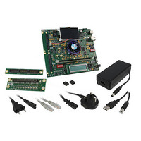
KIT DEV STRATIX IV FPGA 4SE530
Manufacturer
Altera
Series
Stratix® IVr
Type
FPGAr
Datasheet
1.DK-DEV-4SE530N.pdf
(54 pages)
Specifications of DK-DEV-4SE530N
Contents
Board, Cables, CD, DVD, Power Supply
Silicon Manufacturer
Altera
Core Architecture
FPGA
Core Sub-architecture
Stratix
Silicon Core Number
EP4S
Silicon Family Name
Stratix IV E
Rohs Compliant
Yes
For Use With/related Products
EP4SE530
Lead Free Status / RoHS Status
Lead free / RoHS Compliant
Other names
544-2605
Available stocks
Company
Part Number
Manufacturer
Quantity
Price


Chapter 6: Board Test System
Using the Board Test System
© May 2010 Altera Corporation
1
■
■
MAX II Registers
The MAX II registers control allow you to view and change the current MAX II
register values as described in
take effect immediately. For example, writing a 0 to SRST resets the board.
Table 6–1. MAX II Registers
■
■
■
■
Because the Config tab requires that a specific design is running in the FPGA, writing
a 0 to SRST or changing the PSO value can cause the Board Test System to stop
running.
JTAG Chain
The JTAG chain control shows all the devices currently in the JTAG chain. The
Stratix IV E device is always the first device in the chain.
System Reset
(SRST)
Page Select Register
(PSR)
Page Select Override
(PSO)
Page Select Switch
(PSS)
MAX II version—Indicates the version of MAX II code currently running on the
board. The MAX II code resides in the <install
dir>\kits\stratixIVE_4se530_fpga\examples directory. Newer revisions of this
code might be available on the
Altera website.
MAC address—Indicates the MAC address of the board.
Register Name
PSO—Sets the MAX II PSO register. The following options are available:
■
■
PSR—Sets the MAX II PSR register. The numerical values in the list corresponds to
the page of flash memory to load during FPGA reconfiguration. Refer to
for more information.
PSS—Displays the MAX II PSS register value. Refer to
available options.
SRST—Resets the system and reloads the FPGA with a design from flash memory
based on the other MAX II register values. Refer to
Use PSR—Allows the PSR to determine the page of flash memory to use for
FPGA reconfiguration.
Use PSS—Allows the PSS to determine the page of flash memory to use for
FPGA reconfiguration.
Write only
Read / Write
Read / Write
Read only
Read/Write
Capability
Table
Set to 0 to initiate an FPGA reconfiguration.
Determines which of the up to eight (0-7) pages of flash
memory to use for FPGA reconfiguration. The flash memory
ships with pages 0 and 1 preconfigured.
When set to 0, the value in PSR determines the page of
flash memory to use for FPGA reconfiguration. When set to
1, the value in PSS determines the page of flash memory to
use for FPGA reconfiguration.
Holds the current value of the rotary switch (SW5).
Stratix IV E FPGA Development Kit
6–1. Changes to the register values with the GUI
Stratix IV E FPGA Development Kit User Guide
Table 6–1
Description
Table 6–1
for more information.
for the list of
page of the
Table 6–1
6–5
Related parts for DK-DEV-4SE530N
Image
Part Number
Description
Manufacturer
Datasheet
Request
R

Part Number:
Description:
KIT DEV ARRIA II GX FPGA 2AGX125
Manufacturer:
Altera
Datasheet:

Part Number:
Description:
KIT DEV CYCLONE III LS EP3CLS200
Manufacturer:
Altera
Datasheet:

Part Number:
Description:
KIT DEV FPGA 2AGX260 W/6.375G TX
Manufacturer:
Altera
Datasheet:

Part Number:
Description:
KIT DEV MAX V 5M570Z
Manufacturer:
Altera
Datasheet:

Part Number:
Description:
KIT DEV STRATIX V FPGA 5SGXEA7
Manufacturer:
Altera
Datasheet:

Part Number:
Description:
KIT DEVELOPMENT STRATIX III
Manufacturer:
Altera
Datasheet:

Part Number:
Description:
KIT DEVELOPMENT STRATIX IV
Manufacturer:
Altera
Datasheet:

Part Number:
Description:
KIT DEV ARRIA GX 1AGX60N
Manufacturer:
Altera
Datasheet:
Part Number:
Description:
KIT STARTER CYCLONE IV GX
Manufacturer:
Altera
Datasheet:
Part Number:
Description:
KIT DEVELOPMENT STRATIX IV
Manufacturer:
Altera
Datasheet:

Part Number:
Description:
CPLD, EP610 Family, ECMOS Process, 300 Gates, 16 Macro Cells, 16 Reg., 16 User I/Os, 5V Supply, 35 Speed Grade, 24DIP
Manufacturer:
Altera Corporation
Datasheet:
Part Number:
Description:
CPLD, EP610 Family, ECMOS Process, 300 Gates, 16 Macro Cells, 16 Reg., 16 User I/Os, 5V Supply, 15 Speed Grade, 24DIP
Manufacturer:
Altera Corporation
Datasheet: