MPC8360E-RDK Freescale Semiconductor, MPC8360E-RDK Datasheet - Page 86
MPC8360E-RDK
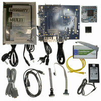
Manufacturer Part Number
MPC8360E-RDK
Description
BOARD REFERENCE DESIGN FOR MPC
Manufacturer
Freescale Semiconductor
Series
PowerQUICC II™ PROr
Type
MPUr
Specifications of MPC8360E-RDK
Contents
Board, Cables, CD, Power Supply
Processor To Be Evaluated
MPC8360E
Data Bus Width
32 bit
Interface Type
RS-232, Ethernet, USB
Operating Supply Voltage
1.3 V
For Use With/related Products
MPC8360E
Lead Free Status / RoHS Status
Lead free / RoHS Compliant


Clocking
Figure 55
The primary clock source for the device can be one of two inputs, CLKIN or PCI_CLK, depending on
whether the device is configured in PCI host or PCI agent mode. Note that in PCI host mode, the primary
clock input also depends on whether PCI clock outputs are selected with RCWH[PCICKDRV]. When the
device is configured as a PCI host device (RCWH[PCIHOST] = 1) and PCI clock output is selected
(RCWH[PCICKDRV] = 1), CLKIN is its primary input clock. CLKIN feeds the PCI clock divider (÷2)
and the multiplexors for PCI_SYNC_OUT and PCI_CLK_OUT. The CFG_CLKIN_DIV configuration
input selects whether CLKIN or CLKIN/2 is driven out on the PCI_SYNC_OUT signal. The
OCCR[PCIOENn] parameters enable the PCI_CLK_OUTn, respectively.
86
CFG_CLKIN_DIV
MPC8360E/MPC8358E PowerQUICC II Pro Processor Revision 2.x TBGA Silicon Hardware Specifications, Rev. 4
CLKIN
shows the internal distribution of clocks within the MPC8358E.
ce_clk to QUICC Engine Block
Engine
QUICC
MPC8358E
PLL
System
Figure 55. MPC8358E Clock Subsystem
PLL
e300 Core
PCI Clock
Clock
Divider
Unit
csb_clk
csb_clk to Rest
of the Device
ddr1_clk
lb_clk
Core PLL
LBIU
/n
DDRC
DLL
core_clk
/2
LCLK[0:2]
LSYNC_OUT
LSYNC_IN
MEMC1_MCK[0:5]
MEMC1_MCK[0:5]
PCI_CLK/
PCI_SYNC_IN
PCI_SYNC_OUT
PCI_CLK_OUT[0:2]
Freescale Semiconductor
Local Bus
Memory
Device
DDRC
Memory
Device
Related parts for MPC8360E-RDK
Image
Part Number
Description
Manufacturer
Datasheet
Request
R

Part Number:
Description:
Mpc8360e Powerquicc Ii Pro Family
Manufacturer:
Freescale Semiconductor, Inc
Datasheet:

Part Number:
Description:
BOARD PROCESSOR FOR MPC8360E
Manufacturer:
Freescale Semiconductor
Datasheet:
Part Number:
Description:
Manufacturer:
Freescale Semiconductor, Inc
Datasheet:
Part Number:
Description:
Manufacturer:
Freescale Semiconductor, Inc
Datasheet:
Part Number:
Description:
Manufacturer:
Freescale Semiconductor, Inc
Datasheet:
Part Number:
Description:
Manufacturer:
Freescale Semiconductor, Inc
Datasheet:
Part Number:
Description:
Manufacturer:
Freescale Semiconductor, Inc
Datasheet:
Part Number:
Description:
Manufacturer:
Freescale Semiconductor, Inc
Datasheet:
Part Number:
Description:
Manufacturer:
Freescale Semiconductor, Inc
Datasheet:
Part Number:
Description:
Manufacturer:
Freescale Semiconductor, Inc
Datasheet:
Part Number:
Description:
Manufacturer:
Freescale Semiconductor, Inc
Datasheet:
Part Number:
Description:
Manufacturer:
Freescale Semiconductor, Inc
Datasheet:
Part Number:
Description:
Manufacturer:
Freescale Semiconductor, Inc
Datasheet:
Part Number:
Description:
Manufacturer:
Freescale Semiconductor, Inc
Datasheet:
Part Number:
Description:
Manufacturer:
Freescale Semiconductor, Inc
Datasheet: