MPC8360E-RDK Freescale Semiconductor, MPC8360E-RDK Datasheet - Page 25
MPC8360E-RDK
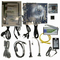
Manufacturer Part Number
MPC8360E-RDK
Description
BOARD REFERENCE DESIGN FOR MPC
Manufacturer
Freescale Semiconductor
Series
PowerQUICC II™ PROr
Type
MPUr
Specifications of MPC8360E-RDK
Contents
Board, Cables, CD, Power Supply
Processor To Be Evaluated
MPC8360E
Data Bus Width
32 bit
Interface Type
RS-232, Ethernet, USB
Operating Supply Voltage
1.3 V
For Use With/related Products
MPC8360E
Lead Free Status / RoHS Status
Lead free / RoHS Compliant


Freescale Semiconductor
At recommended operating conditions with GV
MDQS epilogue end
Notes:
1. The symbols used for timing specifications follow the pattern of t
2. All MCK/MCK referenced measurements are made from the crossing of the two signals ±0.1 V.
3. In the source synchronous mode, MCK/MCK can be shifted in ¼ applied cycle increments through the clock control register.
4. ADDR/CMD includes all DDR SDRAM output signals except MCK/MCK, MCS, and MDQ/MECC/MDM/MDQS. For the
5. Note that t
6. Determined by maximum possible skew between a data strobe (MDQS) and any corresponding bit of data (MDQ), ECC
7. All outputs are referenced to the rising edge of MCK(n) at the pins of the device. Note that t
8. AC timing values are based on the DDR data rate, which is twice the DDR memory bus frequency.
9. In rev. 2.0 silicon, t
inputs and t
(DD) from the rising or falling edge of the reference clock (KH or KL) until the output went invalid (AX or DX). For example,
t
(A) are setup (S) or output valid time. Also, t
(K) goes low (L) until data outputs (D) are invalid (X) or data output hold time.
For the skew measurements referenced for t
address/command valid with the rising edge of MCK.
ADDR/CMD setup and hold specifications, it is assumed that the clock control register is set to adjust the memory clocks by
½ applied cycle.
from the rising edge of the MCK(n) clock (KH) until the MDQS signal is valid (MH). t
of the DQSS override bits in the TIMING_CFG_2 register. In source synchronous mode, this will typically be set to the same
delay as the clock adjust in the CLK_CNTL register. The timing parameters listed in the table assume that these two
parameters have been set to the same adjustment value. See the MPC8360E PowerQUICC II Pro Integrated
Communications Processor Family Reference Manual for a description and understanding of the timing modifications
enabled by use of these bits.
(MECC), or data mask (MDM). The data strobe should be centered inside of the data eye at the pins of the device.
conventions described in note 1.
–0.9 ns. Refer to Errata DDR18 in Chip Errata for the MPC8360E, Rev. 1 .
MPC8360E/MPC8358E PowerQUICC II Pro Processor Revision 2.x TBGA Silicon Hardware Specifications, Rev. 4
DDKHAS
symbolizes DDR timing (DD) for the time t
DDKHMH
(first two letters of functional block)(reference)(state)(signal)(state)
Table 21. DDR and DDR2 SDRAM Output AC Timing Specifications for Source
DDKHMH
follows the symbol conventions described in note 1. For example, t
Parameter
maximum meets the specification of 0.6 ns. In rev. 2.0 silicon, due to errata, t
8
DD
Synchronous Mode (continued)
of (1.8 V or 2.5 V) ± 5%.
DDKLDX
AOSKEW
MCK
symbolizes DDR timing (DD) for the time t
it is assumed that the clock adjustment is set to align the
memory clock reference (K) goes from the high (H) state until outputs
Symbol
t
DDKHME
1
(first two letters of functional block)(signal)(state)(reference)(state)
for outputs. Output hold time can be read as DDR timing
–0.6
Min
DDKHMH
DDKHMH
can be modified through control
DDKHMP
describes the DDR timing (DD)
Max
MCK
0.9
memory clock reference
follows the symbol
DDR and DDR2 SDRAM
DDKHMH
Unit
ns
minimum is
Notes
for
7
25
Related parts for MPC8360E-RDK
Image
Part Number
Description
Manufacturer
Datasheet
Request
R

Part Number:
Description:
Mpc8360e Powerquicc Ii Pro Family
Manufacturer:
Freescale Semiconductor, Inc
Datasheet:

Part Number:
Description:
BOARD PROCESSOR FOR MPC8360E
Manufacturer:
Freescale Semiconductor
Datasheet:
Part Number:
Description:
Manufacturer:
Freescale Semiconductor, Inc
Datasheet:
Part Number:
Description:
Manufacturer:
Freescale Semiconductor, Inc
Datasheet:
Part Number:
Description:
Manufacturer:
Freescale Semiconductor, Inc
Datasheet:
Part Number:
Description:
Manufacturer:
Freescale Semiconductor, Inc
Datasheet:
Part Number:
Description:
Manufacturer:
Freescale Semiconductor, Inc
Datasheet:
Part Number:
Description:
Manufacturer:
Freescale Semiconductor, Inc
Datasheet:
Part Number:
Description:
Manufacturer:
Freescale Semiconductor, Inc
Datasheet:
Part Number:
Description:
Manufacturer:
Freescale Semiconductor, Inc
Datasheet:
Part Number:
Description:
Manufacturer:
Freescale Semiconductor, Inc
Datasheet:
Part Number:
Description:
Manufacturer:
Freescale Semiconductor, Inc
Datasheet:
Part Number:
Description:
Manufacturer:
Freescale Semiconductor, Inc
Datasheet:
Part Number:
Description:
Manufacturer:
Freescale Semiconductor, Inc
Datasheet:
Part Number:
Description:
Manufacturer:
Freescale Semiconductor, Inc
Datasheet: