C8051F326DK Silicon Laboratories Inc, C8051F326DK Datasheet - Page 79
C8051F326DK
Manufacturer Part Number
C8051F326DK
Description
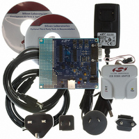
KIT DEV FOR C8051F326/7
Manufacturer
Silicon Laboratories Inc
Type
MCUr
Specifications of C8051F326DK
Contents
Evaluation Board, Power Supply, USB Cables, Adapter and Documentation
Processor To Be Evaluated
C8051F326/F327
Interface Type
USB
Silicon Manufacturer
Silicon Labs
Core Architecture
8051
Silicon Core Number
C8051F326
Silicon Family Name
C8051F32x
Lead Free Status / RoHS Status
Contains lead / RoHS non-compliant
For Use With/related Products
Silicon Laboratories C8051F326, C8051F327
Lead Free Status / Rohs Status
Lead free / RoHS Compliant
Other names
336-1306


11. Port Input/Output
On-Chip digital resources are available through 15 I/O pins. Port pins are organized as shown in
Figure 11.1. Each of the Port pins can be used as general-purpose I/O (GPIO). Some port pins can be
dedicated to special signals such as /SYSCLK, UART TX and RX, and XTAL2 external clock input.
All Port I/Os are 5 V tolerant (refer to Figure 11.2 for the Port cell circuit). The Port I/O cells are configured
as either push-pull or open-drain in the Port Output Mode registers (PnMDOUT, where n = 0,2,3). Com-
plete Electrical Specifications for Port I/O are given in Table 11.1 on page 85.
/SYSCLK
P0.0
P0.1
P0.2
P0.3
P0.4
P0.5
P0.6
P0.7
P2.0
P2.5
P3.0
UART
XTAL2
/INT0
/INT0
C2D
Figure 11.1. Port I/O Functional Block Diagram
GPIOCN.0
TMOD.3
TMOD.3
2
6
MUX
(P0.0 - OUT)
(P0.0 - IN)
Rev. 1.1
(P0.4 - OUT)
(P0.4 - IN)
(P0.5 - OUT)
(P0.5 - IN)
Cells
Cells
Cell
Cell
Cell
Cell
Cell
Cell
Cell
I/O
I/O
I/O
I/O
I/O
I/O
I/O
I/O
I/O
C8051F326/7
P0.0
P0.1
P0.2
P0.3
P0.4
P0.5
P0.6
P0.7
P2.0
P2.5
P3.0
79
Related parts for C8051F326DK
Image
Part Number
Description
Manufacturer
Datasheet
Request
R

Part Number:
Description:
SMD/C°/SINGLE-ENDED OUTPUT SILICON OSCILLATOR
Manufacturer:
Silicon Laboratories Inc
Part Number:
Description:
Manufacturer:
Silicon Laboratories Inc
Datasheet:
Part Number:
Description:
N/A N/A/SI4010 AES KEYFOB DEMO WITH LCD RX
Manufacturer:
Silicon Laboratories Inc
Datasheet:
Part Number:
Description:
N/A N/A/SI4010 SIMPLIFIED KEY FOB DEMO WITH LED RX
Manufacturer:
Silicon Laboratories Inc
Datasheet:
Part Number:
Description:
N/A/-40 TO 85 OC/EZLINK MODULE; F930/4432 HIGH BAND (REV E/B1)
Manufacturer:
Silicon Laboratories Inc
Part Number:
Description:
EZLink Module; F930/4432 Low Band (rev e/B1)
Manufacturer:
Silicon Laboratories Inc
Part Number:
Description:
I°/4460 10 DBM RADIO TEST CARD 434 MHZ
Manufacturer:
Silicon Laboratories Inc
Part Number:
Description:
I°/4461 14 DBM RADIO TEST CARD 868 MHZ
Manufacturer:
Silicon Laboratories Inc
Part Number:
Description:
I°/4463 20 DBM RFSWITCH RADIO TEST CARD 460 MHZ
Manufacturer:
Silicon Laboratories Inc
Part Number:
Description:
I°/4463 20 DBM RADIO TEST CARD 868 MHZ
Manufacturer:
Silicon Laboratories Inc
Part Number:
Description:
I°/4463 27 DBM RADIO TEST CARD 868 MHZ
Manufacturer:
Silicon Laboratories Inc
Part Number:
Description:
I°/4463 SKYWORKS 30 DBM RADIO TEST CARD 915 MHZ
Manufacturer:
Silicon Laboratories Inc
Part Number:
Description:
N/A N/A/-40 TO 85 OC/4463 RFMD 30 DBM RADIO TEST CARD 915 MHZ
Manufacturer:
Silicon Laboratories Inc
Part Number:
Description:
I°/4463 20 DBM RADIO TEST CARD 169 MHZ
Manufacturer:
Silicon Laboratories Inc