DEMO9S08DZ60 Freescale Semiconductor, DEMO9S08DZ60 Datasheet - Page 297
DEMO9S08DZ60
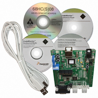
Manufacturer Part Number
DEMO9S08DZ60
Description
BOARD DEMO
Manufacturer
Freescale Semiconductor
Type
MCUr
Datasheets
1.DEMO9S08DZ60.pdf
(416 pages)
2.DEMO9S08DZ60.pdf
(1 pages)
3.DEMO9S08DZ60.pdf
(16 pages)
4.DEMO9S08DZ60.pdf
(2 pages)
5.DEMO9S08DZ60.pdf
(1 pages)
Specifications of DEMO9S08DZ60
Contents
Board, Cable, CD
Processor To Be Evaluated
MC9S08DZ60
Interface Type
RS-232, USB
Silicon Manufacturer
Freescale
Core Architecture
HCS08
Core Sub-architecture
HCS08
Silicon Core Number
MC9S08
Silicon Family Name
S08D
Kit Contents
MC9S08DZ60 Board, Software, Cables, Connectors
Rohs Compliant
Yes
For Use With/related Products
MC9S08DZ60
Lead Free Status / RoHS Status
Lead free / RoHS Compliant


14.2.4
This register has eight read-only status flags. Writes have no effect. Special software sequences (which do
not involve writing to this register) are used to clear these status flags.
Freescale Semiconductor
Reset
Field
RWU
SBK
RE
TE
3
2
1
0
W
R
TDRE
SCI Status Register 1 (SCIxS1)
Transmitter Enable
0 Transmitter off.
1 Transmitter on.
TE must be 1 in order to use the SCI transmitter. When TE = 1, the SCI forces the TxD pin to act as an output
for the SCI system.
When the SCI is configured for single-wire operation (LOOPS = RSRC = 1), TXDIR controls the direction of
traffic on the single SCI communication line (TxD pin).
TE also can be used to queue an idle character by writing TE = 0 then TE = 1 while a transmission is in progress.
Refer to
When TE is written to 0, the transmitter keeps control of the port TxD pin until any data, queued idle, or queued
break character finishes transmitting before allowing the pin to revert to a general-purpose I/O pin.
Receiver Enable — When the SCI receiver is off, the RxD pin reverts to being a general-purpose port I/O pin.
If LOOPS = 1 the RxD pin reverts to being a general-purpose I/O pin even if RE = 1.
0 Receiver off.
1 Receiver on.
Receiver Wakeup Control — This bit can be written to 1 to place the SCI receiver in a standby state where it
waits for automatic hardware detection of a selected wakeup condition. The wakeup condition is either an idle
line between messages (WAKE = 0, idle-line wakeup), or a logic 1 in the most significant data bit in a character
(WAKE = 1, address-mark wakeup). Application software sets RWU and (normally) a selected hardware
condition automatically clears RWU. Refer to
0 Normal SCI receiver operation.
1 SCI receiver in standby waiting for wakeup condition.
Send Break — Writing a 1 and then a 0 to SBK queues a break character in the transmit data stream. Additional
break characters of 10 or 11 (13 or 14 if BRK13 = 1) bit times of logic 0 are queued as long as SBK = 1.
Depending on the timing of the set and clear of SBK relative to the information currently being transmitted, a
second break character may be queued before software clears SBK. Refer to
Queued
0 Normal transmitter operation.
1 Queue break character(s) to be sent.
1
7
Section 14.3.2.1, “Send Break and Queued
Idle” for more details.
= Unimplemented or Reserved
TC
1
6
Table 14-5. SCIxC2 Field Descriptions (continued)
Figure 14-8. SCI Status Register 1 (SCIxS1)
MC9S08DZ60 Series Data Sheet, Rev. 4
RDRF
0
5
IDLE
Section 14.3.3.2, “Receiver Wakeup
0
4
Description
Idle” for more details.
Chapter 14 Serial Communications Interface (S08SCIV4)
OR
3
0
NF
0
2
Section 14.3.2.1, “Send Break and
Operation” for more details.
FE
0
1
PF
0
0
297
Related parts for DEMO9S08DZ60
Image
Part Number
Description
Manufacturer
Datasheet
Request
R

Part Number:
Description:
Manufacturer:
Freescale Semiconductor, Inc
Datasheet:
Part Number:
Description:
Manufacturer:
Freescale Semiconductor, Inc
Datasheet:
Part Number:
Description:
Manufacturer:
Freescale Semiconductor, Inc
Datasheet:
Part Number:
Description:
Manufacturer:
Freescale Semiconductor, Inc
Datasheet:
Part Number:
Description:
Manufacturer:
Freescale Semiconductor, Inc
Datasheet:
Part Number:
Description:
Manufacturer:
Freescale Semiconductor, Inc
Datasheet:
Part Number:
Description:
Manufacturer:
Freescale Semiconductor, Inc
Datasheet:
Part Number:
Description:
Manufacturer:
Freescale Semiconductor, Inc
Datasheet:
Part Number:
Description:
Manufacturer:
Freescale Semiconductor, Inc
Datasheet:
Part Number:
Description:
Manufacturer:
Freescale Semiconductor, Inc
Datasheet:
Part Number:
Description:
Manufacturer:
Freescale Semiconductor, Inc
Datasheet:
Part Number:
Description:
Manufacturer:
Freescale Semiconductor, Inc
Datasheet:
Part Number:
Description:
Manufacturer:
Freescale Semiconductor, Inc
Datasheet:
Part Number:
Description:
Manufacturer:
Freescale Semiconductor, Inc
Datasheet:
Part Number:
Description:
Manufacturer:
Freescale Semiconductor, Inc
Datasheet: