DK-MAXII-1270N Altera, DK-MAXII-1270N Datasheet - Page 18
DK-MAXII-1270N
Manufacturer Part Number
DK-MAXII-1270N
Description
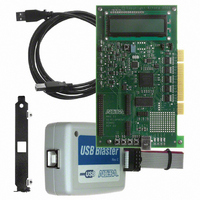
KIT DEV MAXII W/EPM 1270N
Manufacturer
Altera
Series
MAX® IIr
Type
CPLDr
Specifications of DK-MAXII-1270N
Contents
Dev Board, Quartus®II Web Edition, Nios®II Web Edition, Cables, Accessories, Reference Designs and Demos
Silicon Manufacturer
Altera
Core Architecture
CPLD
Core Sub-architecture
MAX
Silicon Core Number
EPM
Silicon Family Name
MAX II
Rohs Compliant
Yes
For Use With/related Products
MAX®II CPLDs
Lead Free Status / RoHS Status
Lead free / RoHS Compliant
Other names
544-2380
Available stocks
Company
Part Number
Manufacturer
Quantity
Price


Demo Designs
2–10
MAX II Development Kit Getting Started User Guide
Test 2. Using a Scope to Measure Power-Up Times
1.
2.
3.
4.
5.
Understanding the Results
The most detailed analysis of the power-up character of a MAX II device
comes from viewing probe points during the power-up cycle with a
digital oscilloscope. The development board has a variable core V
time control. This system uses POT1 to vary the MAX II core V
from 80 μs to 150 ms. The on-board test points provide users with an easy
way to examine the ramp time of V
completion time. The ramp time of V
allowing this circuit to match almost any system’s power-up rise time and
analyze how the MAX II device performs. To make power cycling even
easier, S5 will power cycle the MAX II V
pressed and released. The development board provides four useful probe
points:
■
■
■
■
configured. Press S2 and the 000 changes to the number of times that
the MAX II device could have configured itself in that interval
(typical values should be between 300-600 for fast button pushers).
Program the MAX II device with the InstantOnDemo.pof file that is
located in the <root>/Examples/HW/Demos directory. (Refer to
“Programming the MAX II Device” on page 2–4
to load POF files into the MAX II device.)
Attach scope probes to the four Active I/O test points located near
the prototyping area on the board.
Set the trigger on the scope to the channel connected to the V
test point and trigger on the rising edge (LVTTL logic level).
Set the load on V
resistor (potentiometer), labeled POT1.
Press S5 on the board to interrupt the power and observe the ramp
time of V
below (see
V_INT = V
V_IO = V
GND = Board Ground plane
ACTIVE_IO = MAX II User I/O pin P12
Development Kit Version 1.1.0
CCINT
CCIO
CCINT
Figure
(MAX II I/O voltage supply)
via the provided test point. A sample screen is shown
(MAX II core voltage supply)
CCINT
2–4).
to the desired amount by tuning the variable
CCINT
CCINT
CCINT
and the resulting configuration
can be varied with POT1, thus
supply any time it is
for details on how
Altera Corporation
CC
July 2005
rise time
CCINT
CC
rise
Related parts for DK-MAXII-1270N
Image
Part Number
Description
Manufacturer
Datasheet
Request
R

Part Number:
Description:
KIT DEV MAX V 5M570Z
Manufacturer:
Altera
Datasheet:

Part Number:
Description:
CYCLONE II STARTER KIT EP2C20N
Manufacturer:
Altera
Datasheet:


Part Number:
Description:
CPLD, EP610 Family, ECMOS Process, 300 Gates, 16 Macro Cells, 16 Reg., 16 User I/Os, 5V Supply, 35 Speed Grade, 24DIP
Manufacturer:
Altera Corporation
Datasheet:
Part Number:
Description:
CPLD, EP610 Family, ECMOS Process, 300 Gates, 16 Macro Cells, 16 Reg., 16 User I/Os, 5V Supply, 15 Speed Grade, 24DIP
Manufacturer:
Altera Corporation
Datasheet:
Part Number:
Description:
Manufacturer:
Altera Corporation
Datasheet:
Part Number:
Description:
CPLD, EP610 Family, ECMOS Process, 300 Gates, 16 Macro Cells, 16 Reg., 16 User I/Os, 5V Supply, 30 Speed Grade, 24DIP
Manufacturer:
Altera Corporation
Datasheet:
Part Number:
Description:
High-performance, low-power erasable programmable logic devices with 8 macrocells, 10ns
Manufacturer:
Altera Corporation
Datasheet:
Part Number:
Description:
High-performance, low-power erasable programmable logic devices with 8 macrocells, 7ns
Manufacturer:
Altera Corporation
Datasheet:
Part Number:
Description:
Classic EPLD
Manufacturer:
Altera Corporation
Datasheet:
Part Number:
Description:
High-performance, low-power erasable programmable logic devices with 8 macrocells, 10ns
Manufacturer:
Altera Corporation
Datasheet:
Part Number:
Description:
Manufacturer:
Altera Corporation
Datasheet:
Part Number:
Description:
Manufacturer:
Altera Corporation
Datasheet:
Part Number:
Description:
Manufacturer:
Altera Corporation
Datasheet: