P0037 Terasic Technologies Inc, P0037 Datasheet - Page 16
P0037
Manufacturer Part Number
P0037
Description
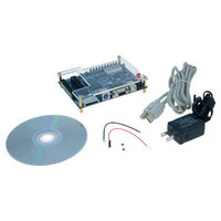
BOARD DEV/EDUCATION ALTERA DE0
Manufacturer
Terasic Technologies Inc
Type
FPGAr
Datasheet
1.EP3C5F256C8N.pdf
(34 pages)
Specifications of P0037
Contents
Board, Cable, CD, Power Supply
For Use With/related Products
Cyclone III
Lead Free Status / RoHS Status
Lead free / RoHS Compliant


1–16
Table 1–20. Cyclone III Devices PLL Specifications
Cyclone III Device Handbook, Volume 2
f
t
t
t
t
t
t
t
t
t
t
f
Notes to
(1) V
(2) This parameter is limited in the Quartus II software by the I/O maximum frequency. The maximum I/O frequency is different for each I/O standard.
(3) The V
(4) A high input jitter directly affects the PLL output jitter. To have low PLL output clock jitter, you must provide a clean clock source, which is less than 200 ps.
(5) Peak-to-peak jitter with a probability level of 10
(6) With 100 MHz scanclk frequency.
OUT
OUTDUTY
LOCK
DLOCK
OUTJITTER_PERIOD_DEDC LK
OUTJITTER_CCJ _DEDCLK
OUTJITTER_PERIOD_IO
OUTJITTER_CCJ _IO
PLL_PSERR
ARESET
CONF IGPLL
SC ANC LK
(to global clock)
counter K value. Therefore, if the counter K has a value of 2, the frequency reported can be lower than the f
jitter of the PLL, when an input jitter of 30 ps is applied.
CC D_P LL
Table
CO
should always be connected to V
frequency reported by the Quartus II software in the PLL summary section of the compilation report takes into consideration the V
(5)
Symbol
(5)
1–20:
(5)
(5)
PLL output frequency (–6 speed grade)
PLL output frequency (–7 speed grade)
PLL output frequency (–8 speed grade)
Duty cycle for external clock output (when set to 50%)
Time required to lock from end of device configuration
Time required to lock dynamically (after switchover,
reconfiguring any non-post-scale counters/delays or
areset is deasserted)
Dedicated clock output period jitter
F
F
Dedicated clock output cycle-to-cycle jitter
F
F
Regular I/O period jitter
F
F
Regular I/O cycle-to-cycle jitter
F
F
Accuracy of PLL phase shift
Minimum pulse width on areset signal.
Time required to reconfigure scan chains for PLLs
scanclk frequency
OUT
OUT
OUT
OUT
OUT
OUT
OUT
OUT
≥ 100 MHz
< 100 MHz
≥ 100 MHz
< 100 MHz
≥ 100 MHz
< 100 MHz
≥ 100 MHz
< 100 MHz
C CINT
through decoupling capacitor and ferrite bead.
–12
(14 sigma, 99.99999999974404% confidence level). The output jitter specification applies to the intrinsic
(Note 1)
Parameter
(Part 2 of 2)
Chapter 1: Cyclone III Device Data Sheet
© January 2010 Altera Corporation
Min
—
—
—
45
—
—
—
—
—
—
—
—
—
—
—
10
—
—
V CO
specification.
3.5
Switching Characteristics
Typ
—
—
—
50
—
—
—
—
—
—
—
—
—
—
—
—
—
(6)
472.5
402.5
Max
450
300
300
650
650
±50
100
55
30
30
75
75
—
—
1
1
C O
SCANCLK
post-scale
cycles
Unit
MHz
MHz
MHz
MHz
mUI
mUI
mUI
mUI
ms
ms
ps
ps
ps
ps
ps
ns
%
Related parts for P0037
Image
Part Number
Description
Manufacturer
Datasheet
Request
R

Part Number:
Description:
MODULE DIGITAL CAMERA 5MP (D5M)
Manufacturer:
Terasic Technologies Inc
Datasheet:

Part Number:
Description:
DE2-70 CALL FOR ACADEMIC PRICING
Manufacturer:
Terasic Technologies Inc
Datasheet:

Part Number:
Description:
USB BLASTER CABLE
Manufacturer:
Terasic Technologies Inc
Datasheet:

Part Number:
Description:
BOARD ADAPTER HSMC TO GPIO
Manufacturer:
Terasic Technologies Inc
Datasheet:

Part Number:
Description:
BOARD ADAPTER THDB-SUM
Manufacturer:
Terasic Technologies Inc
Datasheet:

Part Number:
Description:
KIT DEV 4.3" LCD TOUCH PANEL
Manufacturer:
Terasic Technologies Inc
Datasheet:

Part Number:
Description:
DAUGHTER BOARD AD/DA GPIO ADA
Manufacturer:
Terasic Technologies Inc

Part Number:
Description:
DAUGHTER BOARD AD/DA HSMC ADA
Manufacturer:
Terasic Technologies Inc

Part Number:
Description:
KIT MAX II MICRO
Manufacturer:
Terasic Technologies Inc
Datasheet:

Part Number:
Description:
BOARD DEV DE1 ALTERA
Manufacturer:
Terasic Technologies Inc
Datasheet:

Part Number:
Description:
DE2 CALL FOR ACADEMIC PRICING
Manufacturer:
Terasic Technologies Inc

Part Number:
Description:
MODULE DIGITAL CAMERA 1.3MP
Manufacturer:
Terasic Technologies Inc
Datasheet:

Part Number:
Description:
SENSOR CMOS 1.3MEGA (FOR P0349)
Manufacturer:
Terasic Technologies Inc
Datasheet:
Part Number:
Description:
MODULE DIGITAL CAMERA 5MP (D5M)
Manufacturer:
Terasic Technologies Inc
Datasheet: