OM11048 NXP Semiconductors, OM11048 Datasheet - Page 21
OM11048
Manufacturer Part Number
OM11048
Description
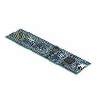
BOARD LPCXPRESSO LPC1343
Manufacturer
NXP Semiconductors
Series
LPCXpressor
Type
MCUr
Datasheet
1.OM11048.pdf
(62 pages)
Specifications of OM11048
Contents
Board, Software
Processor To Be Evaluated
LPC1343
Processor Series
LPC13xx
Interface Type
USB, I2C, UART
Maximum Operating Temperature
+ 85 C
Minimum Operating Temperature
- 40 C
Operating Supply Voltage
3.3 V
Tool Type
Demonstration Board
Core Architecture
ARM
Cpu Core
ARM Cortex M3
Data Bus Width
32 bit
Lead Free Status / RoHS Status
Lead free / RoHS Compliant
For Use With/related Products
LPC1343
Lead Free Status / Rohs Status
Lead free / RoHS Compliant
Other names
568-4947
Available stocks
Company
Part Number
Manufacturer
Quantity
Price

Part Number:
OM11048
Manufacturer:
NXP/恩智浦
Quantity:
20 000
Company:
Part Number:
OM11048Ј¬598
Manufacturer:
PH3
Quantity:
48


NXP Semiconductors
LPC1311_13_42_43
Product data sheet
7.12.1 Features
7.13.1 Features
7.14.1 Features
7.13 10-bit ADC
7.14 General purpose external event counter/timers
The LPC1311/13/42/43 contains one ADC. It is a single 10-bit successive approximation
ADC with eight channels.
The LPC1311/13/42/43 includes two 32-bit counter/timers and two 16-bit counter/timers.
The counter/timer is designed to count cycles of the system derived clock. It can optionally
generate interrupts or perform other actions at specified timer values, based on four
match registers. Each counter/timer also includes one capture input to trap the timer value
when an input signal transitions, optionally generating an interrupt.
•
•
•
•
•
•
•
•
•
•
•
•
•
•
•
•
•
•
•
•
•
The I
pins. The I
Easy to configure as master, slave, or master/slave.
Programmable clocks allow versatile rate control.
Bidirectional data transfer between masters and slaves.
Multi-master bus (no central master).
Arbitration between simultaneously transmitting masters without corruption of serial
data on the bus.
Serial clock synchronization allows devices with different bit rates to communicate via
one serial bus.
Serial clock synchronization can be used as a handshake mechanism to suspend and
resume serial transfer.
The I
The I
10-bit successive approximation ADC.
Input multiplexing among 8 pins.
Power-down mode.
Measurement range 0 V to V
10-bit conversion time ≥ 2.44 μs (up to 400 kSamples/s).
Burst conversion mode for single or multiple inputs.
Optional conversion on transition of input pin or timer match signal.
Individual result registers for each ADC channel to reduce interrupt overhead.
A 32-bit/16-bit counter/timer with a programmable 32-bit/16-bit prescaler.
Counter or timer operation.
One capture channel per timer, that can take a snapshot of the timer value when an
input signal transitions. A capture event may also generate an interrupt.
2
2
2
C-bus interface is a standard I
C-bus can be used for test and diagnostic purposes.
C-bus controller supports multiple address recognition and a bus monitor mode.
2
C-bus interface also supports Fast-mode Plus with bit rates up to 1 Mbit/s.
All information provided in this document is subject to legal disclaimers.
Rev. 3 — 10 August 2010
DD
.
2
C-bus compliant interface with true open-drain
32-bit ARM Cortex-M3 microcontroller
LPC1311/13/42/43
© NXP B.V. 2010. All rights reserved.
21 of 62
Related parts for OM11048
Image
Part Number
Description
Manufacturer
Datasheet
Request
R

Part Number:
Description:
NXP Semiconductors designed the LPC2420/2460 microcontroller around a 16-bit/32-bitARM7TDMI-S CPU core with real-time debug interfaces that include both JTAG andembedded trace
Manufacturer:
NXP Semiconductors
Datasheet:

Part Number:
Description:
NXP Semiconductors designed the LPC2458 microcontroller around a 16-bit/32-bitARM7TDMI-S CPU core with real-time debug interfaces that include both JTAG andembedded trace
Manufacturer:
NXP Semiconductors
Datasheet:
Part Number:
Description:
NXP Semiconductors designed the LPC2468 microcontroller around a 16-bit/32-bitARM7TDMI-S CPU core with real-time debug interfaces that include both JTAG andembedded trace
Manufacturer:
NXP Semiconductors
Datasheet:
Part Number:
Description:
NXP Semiconductors designed the LPC2470 microcontroller, powered by theARM7TDMI-S core, to be a highly integrated microcontroller for a wide range ofapplications that require advanced communications and high quality graphic displays
Manufacturer:
NXP Semiconductors
Datasheet:
Part Number:
Description:
NXP Semiconductors designed the LPC2478 microcontroller, powered by theARM7TDMI-S core, to be a highly integrated microcontroller for a wide range ofapplications that require advanced communications and high quality graphic displays
Manufacturer:
NXP Semiconductors
Datasheet:
Part Number:
Description:
The Philips Semiconductors XA (eXtended Architecture) family of 16-bit single-chip microcontrollers is powerful enough to easily handle the requirements of high performance embedded applications, yet inexpensive enough to compete in the market for hi
Manufacturer:
NXP Semiconductors
Datasheet:
Part Number:
Description:
The XA-S3 device is a member of Philips Semiconductors? XA(eXtended Architecture) family of high performance 16-bitsingle-chip microcontrollers
Manufacturer:
NXP Semiconductors
Datasheet:

Part Number:
Description:
The NXP BlueStreak LH75401/LH75411 family consists of two low-cost 16/32-bit System-on-Chip (SoC) devices
Manufacturer:
NXP Semiconductors
Datasheet:
Part Number:
Description:
The NXP LPC3130/3131 combine an 180 MHz ARM926EJ-S CPU core, high-speed USB2
Manufacturer:
NXP Semiconductors
Datasheet:
Part Number:
Description:
The NXP LPC3141 combine a 270 MHz ARM926EJ-S CPU core, High-speed USB 2
Manufacturer:
NXP Semiconductors
Part Number:
Description:
The NXP LPC3143 combine a 270 MHz ARM926EJ-S CPU core, High-speed USB 2
Manufacturer:
NXP Semiconductors

Part Number:
Description:
The NXP LPC3152 combines an 180 MHz ARM926EJ-S CPU core, High-speed USB 2
Manufacturer:
NXP Semiconductors
Part Number:
Description:
The NXP LPC3154 combines an 180 MHz ARM926EJ-S CPU core, High-speed USB 2
Manufacturer:
NXP Semiconductors

Part Number:
Description:
Standard level N-channel enhancement mode Field-Effect Transistor (FET) in a plastic package using NXP High-Performance Automotive (HPA) TrenchMOS technology
Manufacturer:
NXP Semiconductors
Datasheet: