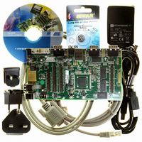
AT91SAM9260-EK Atmel, AT91SAM9260-EK Datasheet - Page 14

AT91SAM9260-EK
Manufacturer Part Number
AT91SAM9260-EK
Description
KIT EVAL FOR AT91SAM9260
Manufacturer
Atmel
Series
AT91SAM Smart ARMr
Type
MCUr
Datasheets
1.AT91SAM9260-EK.pdf
(47 pages)
2.AT91SAM9260-EK.pdf
(39 pages)
3.AT91SAM9260-EK.pdf
(10 pages)
Specifications of AT91SAM9260-EK
Contents
Evaluation Board, Parallel Cable and CD-ROM
Processor To Be Evaluated
AT91SAM9260
Data Bus Width
32 bit
Interface Type
RS-232, Ethernet, USB
Core
ARM 9
Silicon Manufacturer
Atmel
Core Architecture
ARM
Core Sub-architecture
ARM926EJ-S
Silicon Core Number
AT91SAM9260
Silicon Family Name
ARM
Kit Contents
Board, Cables, CD, Power Supply
Rohs Compliant
Yes
For Use With/related Products
AT91SAM9260
Lead Free Status / RoHS Status
Lead free / RoHS Compliant
5.3
6. I/O Line Considerations
6.1
6.2
6.3
14
Programmable I/O Lines Power Supplies
JTAG Port Pins
Test Pin
Reset Pins
AT91SAM9260
The power supplies pins VDDIOM accept two voltage ranges. This allows the device to reach its
maximum speed either out of 1.8V or 3.3V external memories.
The target maximum speed is 100 MHz on the pin SDCK (SDRAM Clock) loaded with 30 pF for
power supply at 1.8V and 50 pF for power supply at 3.3V. The other signals (control, address
and data signals) do not exceed 50 MHz.
The voltage ranges are determined by programming registers in the Chip Configuration registers
located in the Matrix User Interface.
At reset, the selected voltage defaults to 3.3V nominal, and power supply pins can accept either
1.8V or 3.3V. Obviously, the device cannot reach its maximum speed if the voltage supplied to
the pins is 1.8V only. The user must program the EBI voltage range before getting the device out
of its Slow Clock Mode.
TMS, TDI and TCK are Schmitt trigger inputs and have no pull-up resistors.
TDO and RTCK are outputs, driven at up to VDDIOP0, and have no pull-up resistors.
The JTAGSEL pin is used to select the JTAG boundary scan when asserted at a high level (tied
to VDDBU). It integrates a permanent pull-down resistor of about 15 kΩ to GNDBU, so that it can
be left unconnected for normal operations.
The NTRST signal is described in
All the JTAG signals are supplied with VDDIOP0.
The TST pin is used for manufacturing test purposes when asserted high. It integrates a perma-
nent pull-down resistor of about 15 kΩ to GNDBU, so that it can be left unconnected for normal
operations. Driving this line at a high level leads to unpredictable results.
This pin is supplied with VDDBU.
NRST is a bidirectional with an open-drain output integrating a non-programmable pull-up resis-
tor. It can be driven with voltage at up to VDDIOP0.
NTRST is an input which allows reset of the JTAG Test Access port. It has no action on the
processor.
As the product integrates power-on reset cells, which manages the processor and the JTAG
reset, the NRST and NTRST pins can be left unconnected.
The NRST and NTRST pins both integrate a permanent pull-up resistor to VDDIOP0. Its value
can be found in the table “DC Characteristics” in the section “AT91SAM9260 Electrical Charac-
teristics” in the product datasheet.
The NRST signal is inserted in the Boundary Scan.
Section
6.3.
6221JS–ATARM–17-Jul-09


