STEVAL-MKI024V1 STMicroelectronics, STEVAL-MKI024V1 Datasheet - Page 21
STEVAL-MKI024V1
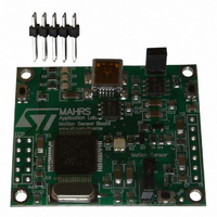
Manufacturer Part Number
STEVAL-MKI024V1
Description
DEMO BOARD BASED ON LIS331DL
Manufacturer
STMicroelectronics
Series
MEMSr
Datasheets
1.STEVAL-MKI024V1.pdf
(42 pages)
2.STEVAL-MKI024V1.pdf
(39 pages)
3.STEVAL-MKI024V1.pdf
(4 pages)
Specifications of STEVAL-MKI024V1
Design Resources
STEVAL-MKI024V1 Gerber Files STEVAL-MKI024V1 Schematics STEVAL-MKI024V1 Bill of Materials
Sensor Type
Accelerometer, 3 Axis
Sensing Range
±2.3g, 9.2g
Interface
SPI, USB
Sensitivity
72mg/digit
Voltage - Supply
5V, USB
Embedded
Yes, MCU, 8-Bit
Utilized Ic / Part
LIS331DL
Acceleration
2 g, 8 g
Sensing Axis
Triple Axis
Output Type
Digital
Interface Type
USB
Silicon Manufacturer
ST Micro
Silicon Core Number
LIS331DL
Kit Application Type
Sensing - Motion / Vibration / Shock
Application Sub Type
Accelerometer
Kit Contents
Board
Lead Free Status / RoHS Status
Lead free / RoHS Compliant
Other names
497-8719
Available stocks
Company
Part Number
Manufacturer
Quantity
Price
Company:

Part Number:
STEVAL-MKI024V1
Manufacturer:
STMicroelectronics
Quantity:
135


LIS331DL
5.2.1
Both the Read Register and Write Register commands are completed in 16 clock pulses or
in multiple of 8 in case of multiple bytes read/write. Bit duration is the time between two
falling edges of SPC. The first bit (bit 0) starts at the first falling edge of SPC after the falling
edge of CS while the last bit (bit 15, bit 23, ...) starts at the last falling edge of SPC just
before the rising edge of CS.
bit 0: RW bit. When 0, the data DI(7:0) is written into the device. When 1, the data DO(7:0)
from the device is read. In latter case, the chip will drive SDO at the start of bit 8.
bit 1: MS bit. When 0, the address will remain unchanged in multiple read/write commands.
When 1, the address will be auto incremented in multiple read/write commands.
bit 2-7: address AD(5:0). This is the address field of the indexed register.
bit 8-15: data DI(7:0) (write mode). This is the data that will be written into the device (MSb
first).
bit 8-15: data DO(7:0) (read mode). This is the data that will be read from the device (MSb
first).
In multiple read/write commands further blocks of 8 clock periods will be added. When MS
bit is 0 the address used to read/write data remains the same for every block. When MS bit
is 1 the address used to read/write data is incremented at every block.
The function and the behavior of SDI and SDO remain unchanged.
SPI read
Figure 7.
The SPI Read command is performed with 16 clock pulses. Multiple byte read command is
performed adding blocks of 8 clock pulses at the previous one.
bit 0: READ bit. The value is 1.
bit 1: MS bit. When 0 do not increment address, when 1 increment address in multiple
reading.
bit 2-7: address AD(5:0). This is the address field of the indexed register.
bit 8-15: data DO(7:0) (read mode). This is the data that will be read from the device (MSb
first).
bit 16-... : data DO(...-8). Further data in multiple byte reading.
SDO
SPC
SPI read protocol
SDI
CS
RW
MS
AD5 AD4 AD3 AD2 AD1 AD0
DO7 DO6 DO5 DO4 DO3 DO2 DO1 DO0
Digital interfaces
21/42
Related parts for STEVAL-MKI024V1
Image
Part Number
Description
Manufacturer
Datasheet
Request
R

Part Number:
Description:
BOARD EVAL FOR MEMS SENSORS
Manufacturer:
STMicroelectronics
Datasheet:

Part Number:
Description:
EVALBOARD/STEVAL-ISV014V1
Manufacturer:
STMicroelectronics
Part Number:
Description:
BOARD EVAL FOR ST802RT1
Manufacturer:
STMicroelectronics
Datasheet:

Part Number:
Description:
BOARD EVAL FOR VACUUM CLEANER
Manufacturer:
STMicroelectronics
Datasheet:

Part Number:
Description:
KIT DEV STARTER ST10F276Z5
Manufacturer:
STMicroelectronics
Datasheet:

Part Number:
Description:
BOARD LED CTLR/DVR STLED316S
Manufacturer:
STMicroelectronics
Datasheet:

Part Number:
Description:
BOARD EVAL BLDC SENSORLESS MOTOR
Manufacturer:
STMicroelectronics
Datasheet:

Part Number:
Description:
BOARD ELECT FISCAL CASH REGISTER
Manufacturer:
STMicroelectronics
Datasheet:

Part Number:
Description:
BOARD EVAL BIPO SOLUTION FOR PFC
Manufacturer:
STMicroelectronics
Datasheet:

Part Number:
Description:
BOARD EVAL UPS 450W VOUT=220V
Manufacturer:
STMicroelectronics
Datasheet:
Part Number:
Description:
STMicroelectronics [RIPPLE-CARRY BINARY COUNTER/DIVIDERS]
Manufacturer:
STMicroelectronics
Datasheet:
Part Number:
Description:
STMicroelectronics [LIQUID-CRYSTAL DISPLAY DRIVERS]
Manufacturer:
STMicroelectronics
Datasheet:
Part Number:
Description:
BOARD EVAL FOR MEMS SENSORS
Manufacturer:
STMicroelectronics
Datasheet: