STEVAL-MKI024V1 STMicroelectronics, STEVAL-MKI024V1 Datasheet - Page 20
STEVAL-MKI024V1
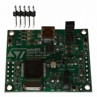
Manufacturer Part Number
STEVAL-MKI024V1
Description
DEMO BOARD BASED ON LIS331DL
Manufacturer
STMicroelectronics
Series
MEMSr
Datasheets
1.STEVAL-MKI024V1.pdf
(42 pages)
2.STEVAL-MKI024V1.pdf
(39 pages)
3.STEVAL-MKI024V1.pdf
(4 pages)
Specifications of STEVAL-MKI024V1
Design Resources
STEVAL-MKI024V1 Gerber Files STEVAL-MKI024V1 Schematics STEVAL-MKI024V1 Bill of Materials
Sensor Type
Accelerometer, 3 Axis
Sensing Range
±2.3g, 9.2g
Interface
SPI, USB
Sensitivity
72mg/digit
Voltage - Supply
5V, USB
Embedded
Yes, MCU, 8-Bit
Utilized Ic / Part
LIS331DL
Acceleration
2 g, 8 g
Sensing Axis
Triple Axis
Output Type
Digital
Interface Type
USB
Silicon Manufacturer
ST Micro
Silicon Core Number
LIS331DL
Kit Application Type
Sensing - Motion / Vibration / Shock
Application Sub Type
Accelerometer
Kit Contents
Board
Lead Free Status / RoHS Status
Lead free / RoHS Compliant
Other names
497-8719
Available stocks
Company
Part Number
Manufacturer
Quantity
Price
Company:

Part Number:
STEVAL-MKI024V1
Manufacturer:
STMicroelectronics
Quantity:
135


Digital interfaces
Table 14.
5.2
20/42
Master
Slave
ST SAD+W
Table 13.
Transfer when Master is receiving (reading) multiple bytes of data from slave
Data are transmitted in byte format (DATA). Each data transfer contains 8 bits. The number
of bytes transferred per transfer is unlimited. Data is transferred with the Most Significant bit
(MSb) first. If a receiver can’t receive another complete byte of data until it has performed
some other function, it can hold the clock line, SCL LOW to force the transmitter into a wait
state. Data transfer only continues when the receiver is ready for another byte and releases
the data line. If a slave receiver doesn’t acknowledge the slave address (i.e. it is not able to
receive because it is performing some real time function) the data line must be left HIGH by
the slave. The Master can then abort the transfer. A LOW to HIGH transition on the SDA line
while the SCL line is HIGH is defined as a STOP condition. Each data transfer must be
terminated by the generation of a STOP (SP) condition.
In order to read multiple bytes, it is necessary to assert the most significant bit of the sub-
address field. In other words, SUB(7) must be equal to 1 while SUB(6-0) represents the
address of first register to be read.
In the presented communication format MAK is Master Acknowledge and NMAK is No
Master Acknowledge.
SPI bus interface
The LIS331DL SPI is a bus slave. The SPI allows to write and read the registers of the
device.
The Serial Interface interacts with the outside world with 4 wires: CS, SPC, SDI and SDO.
Figure 6.
CS is the Serial Port Enable and it is controlled by the SPI master. It goes low at the start of
the transmission and goes back high at the end. SPC is the Serial Port Clock and it is
controlled by the SPI master. It is stopped high when CS is high (no transmission). SDI and
SDO are respectively the Serial Port Data Input and Output. Those lines are driven at the
falling edge of SPC and should be captured at the rising edge of SPC.
Master
Slave
SDO
SPC
SDI
CS
ST
SAK
Transfer when Master is receiving (reading) one byte of data from slave
Read & write protocol
SAD + W
SUB
RW
SAK
MS
AD5 AD4 AD3 AD2 AD1 AD0
SAK
SR SAD+R
SUB
SAK
SAK
SR
DATA
DO7 DO6 DO5 DO4 DO3 DO2 DO1 DO0
DI7 DI6 DI5 DI4 DI3 DI2 DI1 DI0
SAD + R
MAK
DATA
SAK
MAK
DATA
DATA
NMAK
NMAK
LIS331DL
SP
SP
Related parts for STEVAL-MKI024V1
Image
Part Number
Description
Manufacturer
Datasheet
Request
R

Part Number:
Description:
BOARD EVAL FOR MEMS SENSORS
Manufacturer:
STMicroelectronics
Datasheet:

Part Number:
Description:
EVALBOARD/STEVAL-ISV014V1
Manufacturer:
STMicroelectronics
Part Number:
Description:
BOARD EVAL FOR ST802RT1
Manufacturer:
STMicroelectronics
Datasheet:

Part Number:
Description:
BOARD EVAL FOR VACUUM CLEANER
Manufacturer:
STMicroelectronics
Datasheet:

Part Number:
Description:
KIT DEV STARTER ST10F276Z5
Manufacturer:
STMicroelectronics
Datasheet:

Part Number:
Description:
BOARD LED CTLR/DVR STLED316S
Manufacturer:
STMicroelectronics
Datasheet:

Part Number:
Description:
BOARD EVAL BLDC SENSORLESS MOTOR
Manufacturer:
STMicroelectronics
Datasheet:

Part Number:
Description:
BOARD ELECT FISCAL CASH REGISTER
Manufacturer:
STMicroelectronics
Datasheet:

Part Number:
Description:
BOARD EVAL BIPO SOLUTION FOR PFC
Manufacturer:
STMicroelectronics
Datasheet:

Part Number:
Description:
BOARD EVAL UPS 450W VOUT=220V
Manufacturer:
STMicroelectronics
Datasheet:
Part Number:
Description:
STMicroelectronics [RIPPLE-CARRY BINARY COUNTER/DIVIDERS]
Manufacturer:
STMicroelectronics
Datasheet:
Part Number:
Description:
STMicroelectronics [LIQUID-CRYSTAL DISPLAY DRIVERS]
Manufacturer:
STMicroelectronics
Datasheet:
Part Number:
Description:
BOARD EVAL FOR MEMS SENSORS
Manufacturer:
STMicroelectronics
Datasheet: