TMPSNS-RTD1 Microchip Technology, TMPSNS-RTD1 Datasheet - Page 81
TMPSNS-RTD1
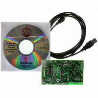
Manufacturer Part Number
TMPSNS-RTD1
Description
BOARD EVAL PT100 RTD TEMP SENSOR
Manufacturer
Microchip Technology
Datasheets
1.MCP3301-CIMS.pdf
(32 pages)
2.PCM18XR1.pdf
(438 pages)
3.MCP6S22DM-PICTL.pdf
(43 pages)
4.TMPSNS-RTD1.pdf
(26 pages)
Specifications of TMPSNS-RTD1
Sensor Type
Temperature
Interface
USB
Embedded
Yes, MCU, 8-Bit
Utilized Ic / Part
MCP3301, MCP6S26, PIC18F2550
Processor To Be Evaluated
MCP6S26, MCP3301, MCP6024, MCP41010, PIC18F2550, TC1071, MCP6002
Data Bus Width
12 bit
Interface Type
USB
Lead Free Status / RoHS Status
Not applicable / Not applicable
Voltage - Supply
-
Sensitivity
-
Sensing Range
-
Lead Free Status / RoHS Status
Lead free / RoHS Compliant, Not applicable / Not applicable


5.6.3
The use of Indexed Literal Offset Addressing mode
effectively changes how the lower portion of Access
RAM (00h to 5Fh) is mapped. Rather than containing
just the contents of the bottom half of Bank 0, this mode
maps the contents from Bank 0 and a user-defined
“window” that can be located anywhere in the data
memory space. The value of FSR2 establishes the
lower boundary of the addresses mapped into the
window, while the upper boundary is defined by FSR2
plus 95 (5Fh). Addresses in the Access RAM above
5Fh are mapped as previously described (see
Section 5.3.3 “Access Bank”). An example of Access
Bank remapping in this addressing mode is shown in
Figure 5-9.
FIGURE 5-9:
© 2009 Microchip Technology Inc.
Example Situation:
Locations in the region
from the FSR2 Pointer
(120h) to the pointer plus
05Fh (17Fh) are mapped
to
Access RAM (000h-05Fh).
Special Function Registers
at F60h through FFFh are
mapped to 60h through
FFh as usual.
Bank 0 addresses below
5Fh are not available in
this mode. They can still
be addressed by using the
BSR.
ADDWF f, d, a
FSR2H:FSR2L = 120h
the
MAPPING THE ACCESS BANK IN
INDEXED LITERAL OFFSET MODE
bottom
of
REMAPPING THE ACCESS BANK WITH INDEXED LITERAL
OFFSET ADDRESSING
the
FFFh
17Fh
F00h
F60h
000h
100h
120h
200h
Data Memory
Bank 14
Bank 15
Window
through
Bank 1
Bank 0
Bank 2
SFRs
PIC18F2455/2550/4455/4550
Remapping of the Access Bank applies only to opera-
tions using the Indexed Literal Offset mode. Operations
that use the BSR (Access RAM bit is ‘1’) will continue
to use Direct Addressing as before. Any indirect or
indexed operation that explicitly uses any of the indirect
file operands (including FSR2) will continue to operate
as standard Indirect Addressing. Any instruction that
uses the Access Bank, but includes a register address
of greater than 05Fh, will use Direct Addressing and
the normal Access Bank map.
5.6.4
Although the Access Bank is remapped when the
extended instruction set is enabled, the operation of the
BSR remains unchanged. Direct Addressing, using the
BSR to select the data memory bank, operates in the
same manner as previously described.
BSR IN INDEXED LITERAL
OFFSET MODE
Bank 1 “Window”
Access Bank
SFRs
DS39632E-page 79
00h
5Fh
60h
FFh
Related parts for TMPSNS-RTD1
Image
Part Number
Description
Manufacturer
Datasheet
Request
R

Part Number:
Description:
Manufacturer:
Microchip Technology Inc.
Datasheet:
Part Number:
Description:
Manufacturer:
Microchip Technology Inc.
Datasheet:
Part Number:
Description:
Manufacturer:
Microchip Technology Inc.
Datasheet:
Part Number:
Description:
Manufacturer:
Microchip Technology Inc.
Datasheet:
Part Number:
Description:
Manufacturer:
Microchip Technology Inc.
Datasheet:
Part Number:
Description:
Manufacturer:
Microchip Technology Inc.
Datasheet:
Part Number:
Description:
Manufacturer:
Microchip Technology Inc.
Datasheet:
Part Number:
Description:
Manufacturer:
Microchip Technology Inc.
Datasheet: