TMPSNS-RTD1 Microchip Technology, TMPSNS-RTD1 Datasheet - Page 14
TMPSNS-RTD1
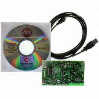
Manufacturer Part Number
TMPSNS-RTD1
Description
BOARD EVAL PT100 RTD TEMP SENSOR
Manufacturer
Microchip Technology
Datasheets
1.MCP3301-CIMS.pdf
(32 pages)
2.PCM18XR1.pdf
(438 pages)
3.MCP6S22DM-PICTL.pdf
(43 pages)
4.TMPSNS-RTD1.pdf
(26 pages)
Specifications of TMPSNS-RTD1
Sensor Type
Temperature
Interface
USB
Embedded
Yes, MCU, 8-Bit
Utilized Ic / Part
MCP3301, MCP6S26, PIC18F2550
Processor To Be Evaluated
MCP6S26, MCP3301, MCP6024, MCP41010, PIC18F2550, TC1071, MCP6002
Data Bus Width
12 bit
Interface Type
USB
Lead Free Status / RoHS Status
Not applicable / Not applicable
Voltage - Supply
-
Sensitivity
-
Sensing Range
-
Lead Free Status / RoHS Status
Lead free / RoHS Compliant, Not applicable / Not applicable


PIC18F2455/2550/4455/4550
TABLE 1-2:
DS39632E-page 12
MCLR/V
OSC1/CLKI
OSC2/CLKO/RA6
Legend: TTL = TTL compatible input
Note 1:
MCLR
V
RE3
OSC1
CLKI
OSC2
CLKO
RA6
PP
2:
Pin Name
PP
/RE3
ST = Schmitt Trigger input with CMOS levels
O
Alternate assignment for CCP2 when CCP2MX Configuration bit is cleared.
Default assignment for CCP2 when CCP2MX Configuration bit is set.
= Output
PIC18F2455/2550 PINOUT I/O DESCRIPTIONS
Number
PDIP,
SOIC
Pin
10
1
9
Type
Pin
I/O
O
O
P
I
I
I
I
Analog
Analog
Buffer
Type
TTL
ST
ST
—
—
Master Clear (input) or programming voltage (input).
Oscillator crystal or external clock input.
Oscillator crystal or clock output.
Master Clear (Reset) input. This pin is an active-low
Reset to the device.
Programming voltage input.
Digital input.
Oscillator crystal input or external clock source input.
External clock source input. Always associated with pin
function OSC1. (See OSC2/CLKO pin.)
Oscillator crystal output. Connects to crystal or resonator in
Crystal Oscillator mode.
In select modes, OSC2 pin outputs CLKO which has 1/4 the
frequency of OSC1 and denotes the instruction cycle rate.
General purpose I/O pin.
CMOS = CMOS compatible input or output
I
P
= Input
= Power
Description
© 2009 Microchip Technology Inc.
Related parts for TMPSNS-RTD1
Image
Part Number
Description
Manufacturer
Datasheet
Request
R

Part Number:
Description:
Manufacturer:
Microchip Technology Inc.
Datasheet:
Part Number:
Description:
Manufacturer:
Microchip Technology Inc.
Datasheet:
Part Number:
Description:
Manufacturer:
Microchip Technology Inc.
Datasheet:
Part Number:
Description:
Manufacturer:
Microchip Technology Inc.
Datasheet:
Part Number:
Description:
Manufacturer:
Microchip Technology Inc.
Datasheet:
Part Number:
Description:
Manufacturer:
Microchip Technology Inc.
Datasheet:
Part Number:
Description:
Manufacturer:
Microchip Technology Inc.
Datasheet:
Part Number:
Description:
Manufacturer:
Microchip Technology Inc.
Datasheet: