TMPSNS-RTD1 Microchip Technology, TMPSNS-RTD1 Datasheet - Page 139
TMPSNS-RTD1
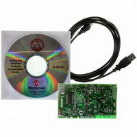
Manufacturer Part Number
TMPSNS-RTD1
Description
BOARD EVAL PT100 RTD TEMP SENSOR
Manufacturer
Microchip Technology
Datasheets
1.MCP3301-CIMS.pdf
(32 pages)
2.PCM18XR1.pdf
(438 pages)
3.MCP6S22DM-PICTL.pdf
(43 pages)
4.TMPSNS-RTD1.pdf
(26 pages)
Specifications of TMPSNS-RTD1
Sensor Type
Temperature
Interface
USB
Embedded
Yes, MCU, 8-Bit
Utilized Ic / Part
MCP3301, MCP6S26, PIC18F2550
Processor To Be Evaluated
MCP6S26, MCP3301, MCP6024, MCP41010, PIC18F2550, TC1071, MCP6002
Data Bus Width
12 bit
Interface Type
USB
Lead Free Status / RoHS Status
Not applicable / Not applicable
Voltage - Supply
-
Sensitivity
-
Sensing Range
-
Lead Free Status / RoHS Status
Lead free / RoHS Compliant, Not applicable / Not applicable


13.0
The Timer2 module timer incorporates the following
features:
• 8-bit Timer and Period registers (TMR2 and PR2,
• Readable and writable (both registers)
• Software programmable prescaler (1:1, 1:4 and
• Software programmable postscaler (1:1 through
• Interrupt on TMR2 to PR2 match
• Optional use as the shift clock for the MSSP
The module is controlled through the T2CON register
(Register 13-1) which enables or disables the timer and
configures the prescaler and postscaler. Timer2 can be
shut off by clearing control bit, TMR2ON (T2CON<2>),
to minimize power consumption.
A simplified block diagram of the module is shown in
Figure 13-1.
REGISTER 13-1:
© 2009 Microchip Technology Inc.
bit 7
Legend:
R = Readable bit
-n = Value at POR
bit 7
bit 6-3
bit 2
bit 1-0
respectively)
1:16)
1:16)
module
U-0
—
TIMER2 MODULE
Unimplemented: Read as ‘0’
T2OUTPS3:T2OUTPS0: Timer2 Output Postscale Select bits
0000 = 1:1 Postscale
0001 = 1:2 Postscale
•
•
•
1111 = 1:16 Postscale
TMR2ON: Timer2 On bit
1 = Timer2 is on
0 = Timer2 is off
T2CKPS1:T2CKPS0: Timer2 Clock Prescale Select bits
00 = Prescaler is 1
01 = Prescaler is 4
1x = Prescaler is 16
T2OUTPS3
R/W-0
T2CON: TIMER2 CONTROL REGISTER
W = Writable bit
‘1’ = Bit is set
T2OUTPS2
R/W-0
PIC18F2455/2550/4455/4550
T2OUTPS1 T2OUTPS0
R/W-0
U = Unimplemented bit, read as ‘0’
‘0’ = Bit is cleared
R/W-0
13.1
In normal operation, TMR2 is incremented from 00h on
each clock (F
clock input gives direct input, divide-by-4 and divide-by-
16 prescale options. These are selected by the prescaler
control bits, T2CKPS1:T2CKPS0 (T2CON<1:0>). The
value of TMR2 is compared to that of the Period register,
PR2, on each clock cycle. When the two values match,
the comparator generates a match signal as the timer
output. This signal also resets the value of TMR2 to 00h
on the next cycle and drives the output counter/post-
scaler (see Section 13.2 “Timer2 Interrupt”).
The TMR2 and PR2 registers are both directly readable
and writable. The TMR2 register is cleared on any
device Reset, while the PR2 register initializes at FFh.
Both the prescaler and postscaler counters are cleared
on the following events:
• a write to the TMR2 register
• a write to the T2CON register
• any device Reset (Power-on Reset, MCLR Reset,
TMR2 is not cleared when T2CON is written.
Watchdog Timer Reset or Brown-out Reset)
Timer2 Operation
TMR2ON
OSC
R/W-0
/4). A 2-bit counter/prescaler on the
x = Bit is unknown
T2CKPS1
R/W-0
DS39632E-page 137
T2CKPS0
R/W-0
bit 0
Related parts for TMPSNS-RTD1
Image
Part Number
Description
Manufacturer
Datasheet
Request
R

Part Number:
Description:
Manufacturer:
Microchip Technology Inc.
Datasheet:
Part Number:
Description:
Manufacturer:
Microchip Technology Inc.
Datasheet:
Part Number:
Description:
Manufacturer:
Microchip Technology Inc.
Datasheet:
Part Number:
Description:
Manufacturer:
Microchip Technology Inc.
Datasheet:
Part Number:
Description:
Manufacturer:
Microchip Technology Inc.
Datasheet:
Part Number:
Description:
Manufacturer:
Microchip Technology Inc.
Datasheet:
Part Number:
Description:
Manufacturer:
Microchip Technology Inc.
Datasheet:
Part Number:
Description:
Manufacturer:
Microchip Technology Inc.
Datasheet: