TMPSNS-RTD1 Microchip Technology, TMPSNS-RTD1 Datasheet - Page 385
TMPSNS-RTD1
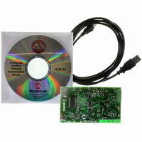
Manufacturer Part Number
TMPSNS-RTD1
Description
BOARD EVAL PT100 RTD TEMP SENSOR
Manufacturer
Microchip Technology
Datasheets
1.MCP3301-CIMS.pdf
(32 pages)
2.PCM18XR1.pdf
(438 pages)
3.MCP6S22DM-PICTL.pdf
(43 pages)
4.TMPSNS-RTD1.pdf
(26 pages)
Specifications of TMPSNS-RTD1
Sensor Type
Temperature
Interface
USB
Embedded
Yes, MCU, 8-Bit
Utilized Ic / Part
MCP3301, MCP6S26, PIC18F2550
Processor To Be Evaluated
MCP6S26, MCP3301, MCP6024, MCP41010, PIC18F2550, TC1071, MCP6002
Data Bus Width
12 bit
Interface Type
USB
Lead Free Status / RoHS Status
Not applicable / Not applicable
Voltage - Supply
-
Sensitivity
-
Sensing Range
-
Lead Free Status / RoHS Status
Lead free / RoHS Compliant, Not applicable / Not applicable


TABLE 28-4:
TABLE 28-5:
© 2009 Microchip Technology Inc.
Operating Conditions: -40°C < T
D313
D314
D315
D316
D317
D318
D319
D320
D321
D322
Operating Conditions: -40°C < T
D323
D324
Note 1:
Param
Param
No.
No.
2:
V
I
V
V
V
V
V
Z
V
V
IL
V
C
If device V
3.0-3.6V supply should be provided on V
This is a recommended maximum for start-up time and in-rush considerations. When the USB regulator is
disabled, there is no maximum.
USB
OUT
OL
OH
ILUSB
IHUSB
CRS
DIFS
CM
Sym
USBANA
USB
Sym
USB MODULE SPECIFICATIONS
USB INTERNAL VOLTAGE REGULATOR SPECIFICATIONS
USB Voltage
Input Leakage on D+ and D-
pins
Input Low Voltage for USB
Buffer
Input High Voltage for USB
Buffer
Crossover Voltage
Differential Input Sensitivity
Differential Common Mode
Range
Driver Output Impedance
Voltage Output Low
Voltage Output High
Regulator Output Voltage
External Filter Capacitor
Value (V
DD
is less than 4.0V, the internal USB voltage regulator should be disabled and an external
Characteristic
Characteristics
USB
A
A
to V
< +85°C (unless otherwise stated).
< +85°C (unless otherwise stated).
SS
)
PIC18F2455/2550/4455/4550
USB
Min
2.0
1.3
0.8
0.0
2.8
3.0
28
—
—
—
0.22
Min
3.0
if the USB module is used.
Typ
—
—
—
—
—
—
—
—
—
0.47
Typ
—
Max
3.6
0.8
2.0
0.2
2.5
0.3
3.6
±1
44
—
12
Max
3.6
(2)
Units
μA
Ω
V
V
V
V
V
V
V
V
Units
μF
V
Voltage on pin must be in this
range for proper USB
operation
V
pin at high-impedance
For V
For V
Voltage range for D+ and D-
crossover to occur
The difference between D+
and D- must exceed this value
while V
1.5 kΩ load connected to 3.6V
15 kΩ load connected to
ground
SS
V
Ceramic or other low-ESR
capacitor recommended
DD
≤ V
USB
USB
> 4.0V
CM
PIN
Comments
range
range
Comments
is met
≤ V
DS39632E-page 383
(1)
DD
;
Related parts for TMPSNS-RTD1
Image
Part Number
Description
Manufacturer
Datasheet
Request
R

Part Number:
Description:
Manufacturer:
Microchip Technology Inc.
Datasheet:
Part Number:
Description:
Manufacturer:
Microchip Technology Inc.
Datasheet:
Part Number:
Description:
Manufacturer:
Microchip Technology Inc.
Datasheet:
Part Number:
Description:
Manufacturer:
Microchip Technology Inc.
Datasheet:
Part Number:
Description:
Manufacturer:
Microchip Technology Inc.
Datasheet:
Part Number:
Description:
Manufacturer:
Microchip Technology Inc.
Datasheet:
Part Number:
Description:
Manufacturer:
Microchip Technology Inc.
Datasheet:
Part Number:
Description:
Manufacturer:
Microchip Technology Inc.
Datasheet: