MCP1726EV Microchip Technology, MCP1726EV Datasheet - Page 5
MCP1726EV
Manufacturer Part Number
MCP1726EV
Description
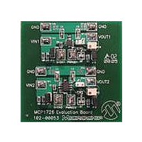
BOARD EVAL FOR MCP1726
Manufacturer
Microchip Technology
Datasheets
1.MCP1726EV.pdf
(2 pages)
2.MCP1726EV.pdf
(30 pages)
3.MCP1726EV.pdf
(24 pages)
4.MCP1726EV.pdf
(4 pages)
5.MCP1726EV.pdf
(24 pages)
Specifications of MCP1726EV
Channels Per Ic
1 - Single
Voltage - Output
0.8 ~ 5V
Current - Output
1A
Voltage - Input
2.3 ~ 6V
Regulator Type
Positive Adjustable
Operating Temperature
-40°C ~ 125°C
Board Type
Fully Populated
Utilized Ic / Part
MCP1726
Processor To Be Evaluated
MCP1726
Silicon Manufacturer
Microchip
Silicon Core Number
MCP1726
Kit Application Type
Power Management - Voltage Regulator
Application Sub Type
LDO
Kit Contents
Board Cables CD Docs
Rohs Compliant
Yes
Lead Free Status / RoHS Status
Contains lead / RoHS non-compliant
Lead Free Status / RoHS Status
Lead free / RoHS Compliant, Contains lead / RoHS non-compliant
Available stocks
Company
Part Number
Manufacturer
Quantity
Price
Company:

Part Number:
MCP1726EV
Manufacturer:
Microchip Technology
Quantity:
135


DC CHARACTERISTICS (CONTINUED)
© 2007 Microchip Technology Inc.
Electrical Specifications: Unless otherwise noted, V
C
Power Good Characteristics
Input Voltage Operating Range
for Valid PWRGD
PWRGD Threshold Voltage
(Referenced to V
PWRGD Output Voltage Low
PWRGD Leakage
PWRGD Time Delay
Detect Threshold to PWRGD
Active Time Delay
Shutdown Input
Logic-High Input
Logic-Low Input
SHDN Input Leakage Current
AC Performance
Output Delay From SHDN
Output Noise
Power Supply Ripple Rejection
Ratio
Thermal Shutdown Temperature
Thermal Shutdown Hysteresis
Note 1:
IN
= C
2:
3:
4:
5:
6:
7:
OUT
Parameters
= 4.7 µF (X7R Ceramic), T
The minimum V
V
voltage for the adjustable cases. V
TCV
temperature range. V
Load regulation is measured at a constant junction temperature using low duty-cycle pulse testing. Load regulation is
tested over a load range from 1 mA to the maximum specified output current.
Dropout voltage is defined as the input-to-output voltage differential at which the output voltage drops 2% below its
nominal value that was measured with an input voltage of V
The maximum allowable power dissipation is a function of ambient temperature, the maximum allowable junction
temperature and the thermal resistance from junction to air. (i.e., T
dissipation will cause the device operating junction temperature to exceed the maximum 150°C rating. Sustained
junction temperatures above 125°C can impact device reliability.
The junction temperature is approximated by soaking the device under test at an ambient temperature equal to the
desired junction temperature. The test time is small enough such that the rise in the junction temperature over the
ambient temperature is not significant.
R
is the nominal regulator output voltage for the fixed cases. V
OUT
OUT
)
= (V
OUT-HIGH
IN
must meet two conditions: V
OUT-LOW
– V
PWRGD_THF
PWRGD_THR
T
V
OUT-LOW
A
V
VDET-PWRGD
P
V
V
PWRGD_VIN
SHDN
SHDN-HIGH
= +25°C. Boldface type applies for junction temperatures, T
PWRGD_L
WRGD
SHDN-Low
PSRR
ΔT
Sym
T
T
T
is the lowest voltage measured over the temperature range.
e
PG
OR
SD
N
SD
_
ILK
R
) *10
LK
= V
6
ADJ *
/ (V
IN
= (V
R
((R
Min
-0.1
1.0
1.2
88
89
89
90
10
45
—
—
—
—
—
—
—
—
—
* ΔTemperature). V
IN
R
1
≥ 2.3V and V
/R
+ 0.5V) or 2.3V, whichever is greater, I
2
)+1).
±0.001
Typ
200
300
170
100
150
0.2
0.1
2.0
92
92
94
93
30
54
10
—
—
Figure
IN
IN
= V
R
4-1.
≥ (V
= 1.2V, 1.8V, etc. V
OUT-HIGH
A
R
, T
+ 0.5V.
Max
+0.1
R
J
6.0
6.0
0.4
96
95
98
96
55
15
—
—
—
—
—
—
—
—
, θ
+ 2.5%) + V
JA
). Exceeding the maximum allowable power
is the highest voltage measured over the
µV/√Hz
Units
%V
%V
µA
ms
ms
µA
dB
µs
µs
µs
°C
°C
%
%
%
%
V
V
DROPOUT.
IN
IN
R
is the desired set point output
OUT
J
T
T
I
V
V
V
V
I
V
C
C
C
V
V
V
SHDN = GND
SHDN = GND to V
V
I
C
V
f = 100 Hz, C
I
V
C
I
V
I
V
(Note 7) of -40°C to +125°C
SINK
PWRGD SINK
OUT
OUT
OUT
OUT
A
A
OUT
OUT
OUT
OUT
PWRGD
DELAY
DELAY
DELAY
IN
IN
IN
OUT
OUT
OUT
INAC
IN
OUT
OUT
MCP1726
= +25°C
= -40°C to +125°C
= 1 mA,
= 2.3V to 6.0V
= 2.3V to 6.0V
= 6V, SHDN =V
= 0 µF
= 200 mA, f = 1 kHz,
= 100 mA,
= 100 µA,
= 100 µA,
= 100 µA
< 2.5V, Falling Edge
> 2.5V, Falling Edge
< 2.5V, Rising Edge
> 2.5V, Rising Edge
= GND to 95% V
= 1 µF (X7R Ceramic),
= 2.5V
= 1.8V, V
= 1.8V, V
= 30 mV pk-pk,
= OPEN
= 0.01 µF
= 0.1 µF
Conditions
= V
DS21936C-page 5
IN
= 1.2 mA
OUT
= 6.0V
IN
IN
= 2.8V
= 2.8V
= 10 µF,
IN
IN
,
R
Related parts for MCP1726EV
Image
Part Number
Description
Manufacturer
Datasheet
Request
R

Part Number:
Description:
Manufacturer:
Microchip Technology Inc.
Datasheet:
Part Number:
Description:
Manufacturer:
Microchip Technology Inc.
Datasheet:
Part Number:
Description:
Manufacturer:
Microchip Technology Inc.
Datasheet:
Part Number:
Description:
Manufacturer:
Microchip Technology Inc.
Datasheet:
Part Number:
Description:
Manufacturer:
Microchip Technology Inc.
Datasheet:
Part Number:
Description:
Manufacturer:
Microchip Technology Inc.
Datasheet:
Part Number:
Description:
Manufacturer:
Microchip Technology Inc.
Datasheet:
Part Number:
Description:
Manufacturer:
Microchip Technology Inc.
Datasheet: