MCP1726EV Microchip Technology, MCP1726EV Datasheet - Page 19
MCP1726EV
Manufacturer Part Number
MCP1726EV
Description
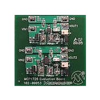
BOARD EVAL FOR MCP1726
Manufacturer
Microchip Technology
Datasheets
1.MCP1726EV.pdf
(2 pages)
2.MCP1726EV.pdf
(30 pages)
3.MCP1726EV.pdf
(24 pages)
4.MCP1726EV.pdf
(4 pages)
5.MCP1726EV.pdf
(24 pages)
Specifications of MCP1726EV
Channels Per Ic
1 - Single
Voltage - Output
0.8 ~ 5V
Current - Output
1A
Voltage - Input
2.3 ~ 6V
Regulator Type
Positive Adjustable
Operating Temperature
-40°C ~ 125°C
Board Type
Fully Populated
Utilized Ic / Part
MCP1726
Processor To Be Evaluated
MCP1726
Silicon Manufacturer
Microchip
Silicon Core Number
MCP1726
Kit Application Type
Power Management - Voltage Regulator
Application Sub Type
LDO
Kit Contents
Board Cables CD Docs
Rohs Compliant
Yes
Lead Free Status / RoHS Status
Contains lead / RoHS non-compliant
Lead Free Status / RoHS Status
Lead free / RoHS Compliant, Contains lead / RoHS non-compliant
Available stocks
Company
Part Number
Manufacturer
Quantity
Price
Company:

Part Number:
MCP1726EV
Manufacturer:
Microchip Technology
Quantity:
135


The maximum power dissipation capability for a
package can be calculated given the junction-to-
ambient thermal resistance and the maximum ambient
temperature for the application. The following equation
can be used to determine the package maximum
internal power dissipation.
EQUATION 5-4:
EQUATION 5-5:
EQUATION 5-6:
© 2007 Microchip Technology Inc.
P
P
T
T
T
T
D(MAX)
D(MAX)
A(MAX)
J(RISE)
J(RISE)
J(MAX)
Rθ
Rθ
T
T
JA
JA
A
J
P
D MAX
= Maximum device power dissipation
= maximum continuous junction
= maximum ambient temperature
= Thermal resistance from junction-to-
= Rise in device junction temperature
= Maximum device power dissipation
= Thermal resistance from junction-to-
= Junction temperature
= Rise in device junction temperature
= Ambient temperature
T
(
J RISE
(
over the ambient temperature
ambient
over the ambient temperature
temperature
ambient
T
)
J
=
)
=
=
(
---------------------------------------------------
T
T
P
J RISE
J MAX
(
(
D MAX
(
Rθ
)
)
+
–
)
JA
×
T
T
A
A MAX
Rθ
(
JA
)
)
5.3
Internal power dissipation, junction temperature rise,
junction temperature and maximum power dissipation
is calculated in the following example. The power dissi-
pation as a result of ground current is small enough to
be neglected.
5.3.1
Device Junction Temperature Rise
The internal junction temperature rise is a function of
internal power dissipation and the thermal resistance
from junction to ambient for the application. The
thermal resistance from junction to ambient (Rθ
derived from an EIA/JEDEC standard for measuring
thermal resistance for small surface-mount packages.
The EIA/JEDEC specification is JESD51-7 “High
Effective Thermal Conductivity Test Board for Leaded
Surface-Mount Packages”. The standard describes the
test method and board specifications for measuring the
thermal resistance from junction to ambient. The actual
thermal resistance for a particular application can vary
depending on many factors such as copper area and
thickness. Refer to AN792, “A Method to Determine
How Much Power a SOT23 Can Dissipate in an Appli-
cation” (DS00792), for more information regarding this
subject.
Package
Input Voltage
LDO Output Voltage and Current
Maximum Ambient Temperature
Internal Power Dissipation
Package Type = 3x3DFN
P
LDO(MAX)
T
T
T
T
J(RISE)
Typical Application
A(MAX)
JRISE
JRISE
V
P
P
I
OUT
OUT
POWER DISSIPATION EXAMPLE
LDO
LDO
V
IN
= 3.3V ± 10%
= 2.5V
= 1.0A
= 70°C
= (V
= (3.3V x 1.1) – (0.975 x 2.5V))
= 1.192 Watts
=
=
=
x 1.0A
IN(MAX)
P
1.192 W x 41.0
48.8
TOTAL
°
– V
C
MCP1726
x Rθ
OUT(MIN)
JA
DS21936C-page 19
°
C/W
) x I
OUT(MAX)
JA
) is
Related parts for MCP1726EV
Image
Part Number
Description
Manufacturer
Datasheet
Request
R

Part Number:
Description:
Manufacturer:
Microchip Technology Inc.
Datasheet:
Part Number:
Description:
Manufacturer:
Microchip Technology Inc.
Datasheet:
Part Number:
Description:
Manufacturer:
Microchip Technology Inc.
Datasheet:
Part Number:
Description:
Manufacturer:
Microchip Technology Inc.
Datasheet:
Part Number:
Description:
Manufacturer:
Microchip Technology Inc.
Datasheet:
Part Number:
Description:
Manufacturer:
Microchip Technology Inc.
Datasheet:
Part Number:
Description:
Manufacturer:
Microchip Technology Inc.
Datasheet:
Part Number:
Description:
Manufacturer:
Microchip Technology Inc.
Datasheet: