MCP1726EV Microchip Technology, MCP1726EV Datasheet - Page 18
MCP1726EV
Manufacturer Part Number
MCP1726EV
Description
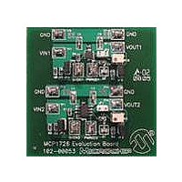
BOARD EVAL FOR MCP1726
Manufacturer
Microchip Technology
Datasheets
1.MCP1726EV.pdf
(2 pages)
2.MCP1726EV.pdf
(30 pages)
3.MCP1726EV.pdf
(24 pages)
4.MCP1726EV.pdf
(4 pages)
5.MCP1726EV.pdf
(24 pages)
Specifications of MCP1726EV
Channels Per Ic
1 - Single
Voltage - Output
0.8 ~ 5V
Current - Output
1A
Voltage - Input
2.3 ~ 6V
Regulator Type
Positive Adjustable
Operating Temperature
-40°C ~ 125°C
Board Type
Fully Populated
Utilized Ic / Part
MCP1726
Processor To Be Evaluated
MCP1726
Silicon Manufacturer
Microchip
Silicon Core Number
MCP1726
Kit Application Type
Power Management - Voltage Regulator
Application Sub Type
LDO
Kit Contents
Board Cables CD Docs
Rohs Compliant
Yes
Lead Free Status / RoHS Status
Contains lead / RoHS non-compliant
Lead Free Status / RoHS Status
Lead free / RoHS Compliant, Contains lead / RoHS non-compliant
Available stocks
Company
Part Number
Manufacturer
Quantity
Price
Company:

Part Number:
MCP1726EV
Manufacturer:
Microchip Technology
Quantity:
135


MCP1726
5.0
5.1
The MCP1726 is used for applications that require high
LDO output current and a power good output.
FIGURE 5-1:
5.1.1
5.2
5.2.1
The internal power dissipation within the MCP1726 is a
function of input voltage, output voltage, output current
and quiescent current. The following equation can be
used to calculate the internal power dissipation for the
LDO.
EQUATION 5-1:
DS21936C-page 18
Off
Input Voltage Range = 3.3V ± 10%
V
V
IN
P
On
V
OUT(MIN)
= 3.3V
LDO
IN(MAX)
C
10 µF
P
Package Type = 3x3DFN8
V
1
APPLICATION CIRCUITS/
ISSUES
Typical Application
V
Power Calculations
LDO
V
IN
=
IN
OUT
APPLICATION CONDITIONS
POWER DISSIPATION
maximum = 3.63V
(
minimum = 2.97V
V
= LDO Pass device internal power
= Maximum input voltage
= LDO minimum output voltage
IN MAX )
1
2
3
4
typical = 2.5V
MCP1726-2.5
(
dissipation
V
V
SHDN
GND PWRGD
I
OUT
IN
IN
)
Typical Application Circuit.
= 1.0A maximum
C
–
DELAY
V
V
V
OUT
OUT
OUT MIN
8
7
6
5
(
)
) I
1000 pF
C
10kΩ
×
3
V
OUT
R
OUT MAX )
1
= 2.5V @ 1A
PWRGD
(
C
10 µF
)
2
In addition to the LDO pass element power dissipation,
there is power dissipation within the MCP1726 as a
result of quiescent or ground current. The power dissi-
pation as a result of the ground current can be
calculated using the following equation:
EQUATION 5-2:
The total power dissipated within the MCP1726 is the
sum of the power dissipated in the LDO pass device
and the P(I
tion, the typical I
Operating at a maximum of 3.63V results in a power
dissipation of 0.51 milli-Watts. For most applications,
this is small compared to the LDO pass device power
dissipation and can be neglected.
The maximum continuous operating junction tempera-
ture specified for the MCP1726 is +125
the internal junction temperature of the MCP1726, the
total internal power dissipation is multiplied by the ther-
mal resistance from junction to ambient (Rθ
device. The thermal resistance from junction to ambi-
ent for the 3x3DFN package is estimated at 41
EQUATION 5-3:
V
P
IN(MAX)
T
P
I(GND)
T
J(MAX)
TOTAL
AMAX
Rθ
I
VIN
JA
T
GND
J MAX
= Power dissipation due to the
= Maximum input voltage
= Current flowing in the V
(
= Maximum continuous junction
= Total device power dissipation
= Thermal resistance from junction-to-
= Maximum ambient temperature
P
quiescent current of the LDO
LDO output current (LDO quiescent
current)
) term. Because of the CMOS construc-
I GND
temperature
ambient
(
)
GND
=
)
P
TOTAL
=
for the MCP1726 is 140 µA.
© 2007 Microchip Technology Inc.
V
IN MAX
(
×
Rθ
)
JA
×
+
I
VIN
T
IN
°
AMAX
C
pin with no
.
To estimate
JA
°
) of the
C/W.
Related parts for MCP1726EV
Image
Part Number
Description
Manufacturer
Datasheet
Request
R

Part Number:
Description:
Manufacturer:
Microchip Technology Inc.
Datasheet:
Part Number:
Description:
Manufacturer:
Microchip Technology Inc.
Datasheet:
Part Number:
Description:
Manufacturer:
Microchip Technology Inc.
Datasheet:
Part Number:
Description:
Manufacturer:
Microchip Technology Inc.
Datasheet:
Part Number:
Description:
Manufacturer:
Microchip Technology Inc.
Datasheet:
Part Number:
Description:
Manufacturer:
Microchip Technology Inc.
Datasheet:
Part Number:
Description:
Manufacturer:
Microchip Technology Inc.
Datasheet:
Part Number:
Description:
Manufacturer:
Microchip Technology Inc.
Datasheet: