MCP1726EV Microchip Technology, MCP1726EV Datasheet - Page 20
MCP1726EV
Manufacturer Part Number
MCP1726EV
Description
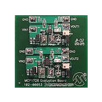
BOARD EVAL FOR MCP1726
Manufacturer
Microchip Technology
Datasheets
1.MCP1726EV.pdf
(2 pages)
2.MCP1726EV.pdf
(30 pages)
3.MCP1726EV.pdf
(24 pages)
4.MCP1726EV.pdf
(4 pages)
5.MCP1726EV.pdf
(24 pages)
Specifications of MCP1726EV
Channels Per Ic
1 - Single
Voltage - Output
0.8 ~ 5V
Current - Output
1A
Voltage - Input
2.3 ~ 6V
Regulator Type
Positive Adjustable
Operating Temperature
-40°C ~ 125°C
Board Type
Fully Populated
Utilized Ic / Part
MCP1726
Processor To Be Evaluated
MCP1726
Silicon Manufacturer
Microchip
Silicon Core Number
MCP1726
Kit Application Type
Power Management - Voltage Regulator
Application Sub Type
LDO
Kit Contents
Board Cables CD Docs
Rohs Compliant
Yes
Lead Free Status / RoHS Status
Contains lead / RoHS non-compliant
Lead Free Status / RoHS Status
Lead free / RoHS Compliant, Contains lead / RoHS non-compliant
Available stocks
Company
Part Number
Manufacturer
Quantity
Price
Company:

Part Number:
MCP1726EV
Manufacturer:
Microchip Technology
Quantity:
135


MCP1726
Junction Temperature Estimate
To estimate the internal junction temperature, the
calculated temperature rise is added to the ambient or
offset temperature. For this example, the worst-case
junction temperature is estimated below:
As you can see from the result, this application will be
operating very near the maximum operating junction
temperature of 125°C. The PCB layout for this
application is very important as it has a significant
impact on the junction-to-ambient thermal resistance
(Rθ
in this application.
Maximum Package Power Dissipation at
70°C Ambient Temperature
From this table you can see the difference in maximum
allowable power dissipation between the 3x3 DFN
package and the 8-pin SOIC package. This difference
is due to the exposed metal tab on the bottom of the
DFN package. The exposed tab of the DFN package
provides a very good thermal path from the die of the
LDO to the PCB. The PCB then acts like a heatsink,
providing more area to distribute the heat generated by
the LDO.
DS21936C-page 20
3x3 DFN (41° C/W Rθ
8LD SOIC (150°C/Watt Rθ
JA
P
P
P
P
) of the 3x3 DFN package, which is very important
D(MAX)
D(MAX)
D(MAX)
D(MAX)
T
T
T
= (125°C – 70°C) / 41° C/W
= 1.34W
= (125°C – 70°C)/ 150° C/W
= 0.366W
J
J
J
=
=
=
JA
)
T
48.8°C + 70.0°C
118.8°C
JRISE
JA
)
+ T
A(MAX)
© 2007 Microchip Technology Inc.
Related parts for MCP1726EV
Image
Part Number
Description
Manufacturer
Datasheet
Request
R

Part Number:
Description:
Manufacturer:
Microchip Technology Inc.
Datasheet:
Part Number:
Description:
Manufacturer:
Microchip Technology Inc.
Datasheet:
Part Number:
Description:
Manufacturer:
Microchip Technology Inc.
Datasheet:
Part Number:
Description:
Manufacturer:
Microchip Technology Inc.
Datasheet:
Part Number:
Description:
Manufacturer:
Microchip Technology Inc.
Datasheet:
Part Number:
Description:
Manufacturer:
Microchip Technology Inc.
Datasheet:
Part Number:
Description:
Manufacturer:
Microchip Technology Inc.
Datasheet:
Part Number:
Description:
Manufacturer:
Microchip Technology Inc.
Datasheet: