STEVAL-ISA056V1 STMicroelectronics, STEVAL-ISA056V1 Datasheet - Page 44
STEVAL-ISA056V1
Manufacturer Part Number
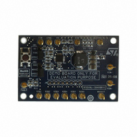
STEVAL-ISA056V1
Description
BOARD EVAL BASED ON PM6600
Manufacturer
STMicroelectronics
Type
PWM Controllersr
Specifications of STEVAL-ISA056V1
Design Resources
STEVAL-ISA056V1 Gerber Files STEVAL-ISA056V1 Schematic STEVAL-ISA056V1 Bill of Material
Current - Output / Channel
30mA
Outputs And Type
6, Non-Isolated
Voltage - Output
36 V
Features
Dimmable
Voltage - Input
4.5 ~ 28V
Utilized Ic / Part
PM6600
Input Voltage
4.5 V to 28 V
Output Voltage
36 V
Product
Power Management Modules
Core Chip
PM6600
Topology
Boost
No. Of Outputs
1
Dimming Control Type
PWM
Mcu Supported Families
PM6600
Lead Free Status / RoHS Status
Lead free / RoHS Compliant
For Use With/related Products
PM6600
Other names
497-8414
Available stocks
Company
Part Number
Manufacturer
Quantity
Price
Company:

Part Number:
STEVAL-ISA056V1
Manufacturer:
STMicroelectronics
Quantity:
1


Layout guidelines
Appendix A
A.1
A.1.1
A.1.2
A.2
44/60
Basic points:
●
●
GNDs planes - 1 device
If the pcb has 2 layers, the PGND area has to be in the top layer, together with the LX area
and the Vin and Vout area, in order to reduce the number of the vias.
The SGND plane is the bottom layer of the board and it is also present near the signal
components on the top layer.
The SGND and PGND connection can be made using the thermal pad of the device.
If the pcb has 4 layers, the PGND and SGND planes must be separated into 2 different
layers. Moreover, they must be connected together in only 1 point, near the PGND pin of the
device. It is recommended to duplicate the LX area into one inner layer, to reduce the
impedance and improve the noise rejection immunity of the device.
If the PM6600 device is mounted on a more complex demonstration board (ex. RGB, multi-
device application, LCD driver + backlight driver board), the PGND and SGND connection
should be present only near the PGND pin of the device. This is relevant in complex
systems because of the possible cross-talking noise between each block of the system.
In order to connect together the PGND and SGND nets, it is not advisable to use a 0 Ω
resistor, because it can produce a voltage drop between the two GNDs planes and it may
damage the device.
It is preferable to connect together the PGND and SGND to the thermal pad of the device, or
with a short pcb trace near the PGND pin of the device.
GNDs planes - 3 devices (RGB)
The SGND plane is the same for all the PM6600 devices – bottom layer (or internal 2-3).
Each PM6600 device must have its own PGND area (top layer), connected to the main
SGND in one point, near the PGND pin of each device > totally 3 connections between the
SGND and PGND, 1 for each driver:
PGND_red - SGND; PGND_blue - SGND; PGND_green - SGND.
Compensation network
The components Rcomp – Ccomp of the compensation network should be as close as
possible to the COMP pin of the device. This permits to avoid any noise issue - instability of
the compensation.
This PCB trace should be designed in the opposite side of the device respect to the power
area (according to the pins position). This subdivision improves the noise rejection of the
system and permits to have a stable loop.
The device thermal pad is SGND.
The device has 2 GND pins: SGND and PGND
Layout guidelines
Doc ID 14248 Rev 7
PM6600
Related parts for STEVAL-ISA056V1
Image
Part Number
Description
Manufacturer
Datasheet
Request
R

Part Number:
Description:
BOARD RGB CTR ST7,STP08C596MTR
Manufacturer:
STMicroelectronics
Datasheet:

Part Number:
Description:
Power Management IC Development Tools Full Speed USB to RS232 Bridge Demo
Manufacturer:
STMicroelectronics
Datasheet:
Part Number:
Description:
Power Management IC Development Tools 2.5W solar eval BRD USB SPV1040 LD39050
Manufacturer:
STMicroelectronics
Datasheet:

Part Number:
Description:
BOARD EVAL FOR MEMS SENSORS
Manufacturer:
STMicroelectronics
Datasheet:

Part Number:
Description:
KIT DEV STARTER ST10F276Z5
Manufacturer:
STMicroelectronics
Datasheet:

Part Number:
Description:
BOARD EVAL HDMI $ VIDEO SWITCH
Manufacturer:
STMicroelectronics
Datasheet:

Part Number:
Description:
BOARD DEMO ACCELEROMETER DIL24
Manufacturer:
STMicroelectronics
Datasheet:

Part Number:
Description:
BOARD STLM75/STDS75/ST72F651
Manufacturer:
STMicroelectronics
Datasheet:

Part Number:
Description:
EVAL BOARD 3AXIS MEMS ACCELLRMTR
Manufacturer:
STMicroelectronics
Datasheet:

Part Number:
Description:
BOARD EVAL 8BIT MICRO + TDE1708
Manufacturer:
STMicroelectronics
Datasheet:
Part Number:
Description:
STMicroelectronics [RIPPLE-CARRY BINARY COUNTER/DIVIDERS]
Manufacturer:
STMicroelectronics
Datasheet:
Part Number:
Description:
STMicroelectronics [LIQUID-CRYSTAL DISPLAY DRIVERS]
Manufacturer:
STMicroelectronics
Datasheet:
Part Number:
Description:
BOARD EVAL FOR MEMS SENSORS
Manufacturer:
STMicroelectronics
Datasheet: