DK86060-3 Fujitsu Semiconductor America Inc, DK86060-3 Datasheet - Page 39
DK86060-3
Manufacturer Part Number
DK86060-3
Description
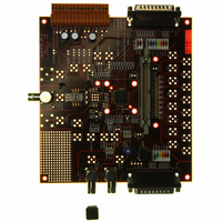
KIT DEV 16BIT DAC FOR MB86060
Manufacturer
Fujitsu Semiconductor America Inc
Specifications of DK86060-3
Number Of Dac's
1
Number Of Bits
16
Outputs And Type
1, Differential
Sampling Rate (per Second)
400M
Data Interface
Parallel
Dac Type
Current
Voltage Supply Source
Single
Operating Temperature
-40°C ~ 85°C
Utilized Ic / Part
MB86060
Lead Free Status / RoHS Status
Lead free / RoHS Compliant
Other names
865-1009


February 2009 Version 2.0
FME/MS/SFDAC1/DS/4250
MB86060 16-bit Interpolating Digital to Analog Converter
Digital Control Interface
Clock Interface
Copyright © 2003-2009 Fujitsu Microelectronics Europe GmbH
Disclaimer: The contents of this document are subject to change without notice. Customers are advised to consult with FUJITSU sales representatives before
32, 36, 65, 69
33, 37, 64, 68
20, 22, 24
Pin Nos.
Pin Nos.
19, 25
61
62
63
73
74
28
75
76
66
71
27
38
39
40
30
26
67
21
23
34
35
17
18
29
3
4
ordering.The information and circuit diagrams in this document are presented “as is”, no license is granted by implication or otherwise.
Pin Name
Pin Name
NSHAPE
CKOUTB
RESETB
CLKSEL
CKOUT
SHUF0
SHUF1
TWOC
DITH0
DITH1
DITH2
OVER
XOUT
CVDD
CSUB
FILTS
OSC0
OSC1
MUL2
MUL1
MUL0
LOCK
CLKB
CVSS
FILTF
VDD
VSS
CLK
N/C
XIN
Output
Output
Power
Power
Power
Power
Input/
Input/
O
O
O
O
O
-
-
I
I
I
I
I
I
I
I
I
I
I
I
I
I
I
I
I
I
I
Programmable Dither control bit 0. See table 6
Programmable Dither control bit 1. See table 6
Programmable Dither control bit 2. See table 6
Slow Interpolation Filter control. See table 5
Fast Interpolation Filter control. See table 5
Noise shaper, ‘1’ = enabled. See section 1.5
Segment Shuffling control bit 0. See table 7.
Segment Shuffling control bit 1. See table 7.
Input data format selection, ‘1’ = 2’s Complement
Digital overflow warning. ‘1’ = overflow condition
Clock Select. Differential clock =’1‘, Crystal clock via XIN = ‘0’
Delay line control bit 0. Internal pull-down resistor. See table 4.
Delay line control bit 1. Internal pull-down resistor. See table 4.
Clock multiplier mode control bit 2. See table 4.
Clock multiplier mode control bit 1. See table 4
Clock multiplier mode control bit 0. See table 4
DLL locked indicator, ’1’ = locked
Device reset, ’0’ = reset
No connection. Do not connect
Digital supply, +3.3V. Decouple to VSS
Digital ground, 0V
Differential input clock (CLK In), negative input.
Differential input clock (CLK In), positive input.
Differential data output clock (Data CLK), negative output.
Differential data output clock (Data CLK), positive output.
Crystal / clock input. Connect to CVSS when not used
Crystal oscillator circuit output
Clock supply, +3.3V. Decouple to CVSS.
Clock ground, 0V
Clock substrate. Link to VSS
Production
Description
Description
Page 39 of 44
Related parts for DK86060-3
Image
Part Number
Description
Manufacturer
Datasheet
Request
R

Part Number:
Description:
IC POWER SUPPLY MONITOR 8SOP
Manufacturer:
Fujitsu Semiconductor America Inc
Datasheet:
Part Number:
Description:
IC POWER SUPPLY MONITOR 8SOP
Manufacturer:
Fujitsu Semiconductor America Inc
Datasheet:

Part Number:
Description:
IC MCU 60K FLASH 2KB RAM 52LQFP
Manufacturer:
Fujitsu Semiconductor America Inc
Datasheet:

Part Number:
Description:
IC MCU 32BIT 256KB FLASH 120LQFP
Manufacturer:
Fujitsu Semiconductor America Inc
Datasheet:
Part Number:
Description:
IC CTLR TOUCH SENSOR 12CH 30SSOP
Manufacturer:
Fujitsu Semiconductor America Inc
Datasheet:

Part Number:
Description:
IC CTLR TOUCH SENSOR 12CH 40QFN
Manufacturer:
Fujitsu Semiconductor America Inc
Datasheet:
Part Number:
Description:
SYNTHESIZER PLL DUAL INP 20SSOP
Manufacturer:
Fujitsu Semiconductor America Inc
Datasheet:

Part Number:
Description:
SYNTHESZR PLL 1.1GHZ DUAL 16SSOP
Manufacturer:
Fujitsu Semiconductor America Inc
Datasheet:

Part Number:
Description:
IC SSCG EMI RED 8-SOIC
Manufacturer:
Fujitsu Semiconductor America Inc
Datasheet:

Part Number:
Description:
IC SSCG EMI RED 8-TSSOP
Manufacturer:
Fujitsu Semiconductor America Inc
Datasheet:

Part Number:
Description:
IC SSCG EMI RED 8-SOP
Manufacturer:
Fujitsu Semiconductor America Inc
Datasheet:

Part Number:
Description:
SYNTHESIZER PLL 2.5GHZ 16SSOP
Manufacturer:
Fujitsu Semiconductor America Inc
Datasheet:
Part Number:
Description:
SYNTHESIZER PLL 1.2GHZ 16SSOP
Manufacturer:
Fujitsu Semiconductor America Inc
Datasheet:

Part Number:
Description:
SYNTHESIZER PLL 2.5GHZ 16BCC
Manufacturer:
Fujitsu Semiconductor America Inc
Datasheet:

Part Number:
Description:
IC SSCG EMI RED 8-SOP
Manufacturer:
Fujitsu Semiconductor America Inc
Datasheet: