DK86060-3 Fujitsu Semiconductor America Inc, DK86060-3 Datasheet - Page 29
DK86060-3
Manufacturer Part Number
DK86060-3
Description
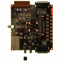
KIT DEV 16BIT DAC FOR MB86060
Manufacturer
Fujitsu Semiconductor America Inc
Specifications of DK86060-3
Number Of Dac's
1
Number Of Bits
16
Outputs And Type
1, Differential
Sampling Rate (per Second)
400M
Data Interface
Parallel
Dac Type
Current
Voltage Supply Source
Single
Operating Temperature
-40°C ~ 85°C
Utilized Ic / Part
MB86060
Lead Free Status / RoHS Status
Lead free / RoHS Compliant
Other names
865-1009


February 2009 Version 2.0
FME/MS/SFDAC1/DS/4250
MB86060 16-bit Interpolating Digital to Analog Converter
4.8
Where signals have to be tracked as differential pairs, attention should be paid to the routing and
positioning of these tracks. Wherever possible, differential tracks should be routed parallel to each
other, and kept as close together as possible for the maximum distance possible. The total length of
each track in a differential pair should be equalised, and the same number of vias should always be
used. Where differential tracks have to diverge to connect to component pins, the distance that the
two tracks are routed separately should be equalised. See figure 18.
Where multiple routing layers are available, differential tracking should be kept on the same layer,
rather than as a stacked pair on adjacent layers. (This may introduce more noise onto one track than
the other due to each track being coupled to different ground planes). Where tracks are routed close
to other signals or noise sources, sufficient separation should be maintained so as to not introduce
significantly more distortion onto one track than the other. Particular attention should be paid to the
positioning of through board vias, which may be exposed to noise from tracking on the layers they
pass through. Switching tracking from one layer to another with vias should be avoided if possible,
but where necessary the vias should be positioned close to each other, within the same plane region
on all layers, and located so as to avoid potential sources of noise on all layers.
Careful attention should be paid to the positioning of signal tracking around plane splits. Signal tracks
must never cross a ground or power plane split, as the return current (which tends to follow the signal
track within the plane) will be forced to follow the plane split around to the star point or until it can find
another way to couple back into the plane on the other side of the split. This can create large ground
current loops within the planes that may interfere with other sections of the application.
Copyright © 2003-2009 Fujitsu Microelectronics Europe GmbH
Disclaimer: The contents of this document are subject to change without notice. Customers are advised to consult with FUJITSU sales representatives before
One via closer to plane
split than other
Signal Routing
A: Poor Differential Tracking Layout
ordering.The information and circuit diagrams in this document are presented “as is”, no license is granted by implication or otherwise.
Figure 18 Differential Tracking Examples
Un-equal net lengths
Via moved away from plane
split and closer together
B: Correct Differential Tracking Layout
Production
Near-equalised net lengths
Page 29 of 44
Related parts for DK86060-3
Image
Part Number
Description
Manufacturer
Datasheet
Request
R

Part Number:
Description:
IC POWER SUPPLY MONITOR 8SOP
Manufacturer:
Fujitsu Semiconductor America Inc
Datasheet:
Part Number:
Description:
IC POWER SUPPLY MONITOR 8SOP
Manufacturer:
Fujitsu Semiconductor America Inc
Datasheet:

Part Number:
Description:
IC MCU 60K FLASH 2KB RAM 52LQFP
Manufacturer:
Fujitsu Semiconductor America Inc
Datasheet:

Part Number:
Description:
IC MCU 32BIT 256KB FLASH 120LQFP
Manufacturer:
Fujitsu Semiconductor America Inc
Datasheet:
Part Number:
Description:
IC CTLR TOUCH SENSOR 12CH 30SSOP
Manufacturer:
Fujitsu Semiconductor America Inc
Datasheet:

Part Number:
Description:
IC CTLR TOUCH SENSOR 12CH 40QFN
Manufacturer:
Fujitsu Semiconductor America Inc
Datasheet:
Part Number:
Description:
SYNTHESIZER PLL DUAL INP 20SSOP
Manufacturer:
Fujitsu Semiconductor America Inc
Datasheet:

Part Number:
Description:
SYNTHESZR PLL 1.1GHZ DUAL 16SSOP
Manufacturer:
Fujitsu Semiconductor America Inc
Datasheet:

Part Number:
Description:
IC SSCG EMI RED 8-SOIC
Manufacturer:
Fujitsu Semiconductor America Inc
Datasheet:

Part Number:
Description:
IC SSCG EMI RED 8-TSSOP
Manufacturer:
Fujitsu Semiconductor America Inc
Datasheet:

Part Number:
Description:
IC SSCG EMI RED 8-SOP
Manufacturer:
Fujitsu Semiconductor America Inc
Datasheet:

Part Number:
Description:
SYNTHESIZER PLL 2.5GHZ 16SSOP
Manufacturer:
Fujitsu Semiconductor America Inc
Datasheet:
Part Number:
Description:
SYNTHESIZER PLL 1.2GHZ 16SSOP
Manufacturer:
Fujitsu Semiconductor America Inc
Datasheet:

Part Number:
Description:
SYNTHESIZER PLL 2.5GHZ 16BCC
Manufacturer:
Fujitsu Semiconductor America Inc
Datasheet:

Part Number:
Description:
IC SSCG EMI RED 8-SOP
Manufacturer:
Fujitsu Semiconductor America Inc
Datasheet: