MCP4728EV Microchip Technology, MCP4728EV Datasheet - Page 5
MCP4728EV
Manufacturer Part Number
MCP4728EV
Description
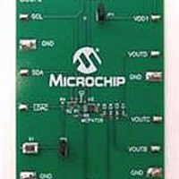
BOARD EVAL 12BIT 4CH DAC MCP4728
Manufacturer
Microchip Technology
Type
D/Ar
Specifications of MCP4728EV
Number Of Dac's
4
Number Of Bits
12
Outputs And Type
1, Single Ended
Data Interface
I²C
Settling Time
6µs
Dac Type
Voltage
Voltage Supply Source
Single
Operating Temperature
-40°C ~ 125°C
Utilized Ic / Part
MCP4728
Product
Data Conversion Development Tools
Resolution
12 bit
Interface Type
I2C
Supply Voltage (max)
5.5 V
Supply Voltage (min)
2.7 V
Silicon Manufacturer
Microchip
Silicon Core Number
MCP4728
Kit Application Type
Data Converter
Application Sub Type
DAC
Kit Contents
Board
For Use With/related Products
MCP4728
Lead Free Status / RoHS Status
Lead free / RoHS Compliant
Lead Free Status / RoHS Status
Lead free / RoHS Compliant, Lead free / RoHS Compliant
Available stocks
Company
Part Number
Manufacturer
Quantity
Price
Company:

Part Number:
MCP4728EV
Manufacturer:
Microchip Technology
Quantity:
135
Company:
Part Number:
MCP4728EV
Manufacturer:
MICROCHIP
Quantity:
12 000


TABLE 1-1:
© 2009 Microchip Technology Inc.
Electrical Specifications: Unless otherwise indicated, all parameters apply at V
R
Full Scale Range
(Note 7)
Output Voltage Settling
Time
Analog Output Time Delay
from Power-Down Mode
Time delay to settle to new
reference
(Note 4)
Power Supply Rejection
Capacitive Load Stability
Slew Rate
Phase Margin
Short Circuit Current
Short Circuit Current
Duration
DC Output Impedance
(Note 4)
Dynamic Performance (Note 4)
Major Code Transition
Glitch
Digital Feedthrough
Analog Crosstalk
DAC-to-DAC Crosstalk
Note 1:
L
= 5 kΩ, C
2:
3:
4:
5:
6:
7:
8:
9:
Parameter
All digital input pins (SDA, SCL, LDAC) are tied to “High”, Output pins are unloaded, code = 0x000.
The power-up ramp rate measures the rise of V
This parameter is ensured by design and not 100% tested.
This parameter is ensured by characterization and not 100% tested.
Test code range: 100 - 4000 codes, V
Time delay to settle to a new reference when switching from external to internal reference or vice versa.
This parameter is indirectly tested by Offset and Gain error testing.
Within 1/2 LSB of the final value when code changes from 1/4 of to 3/4 of full scale.
This time delay is measured from the falling edge of ACK pulse in I
This time delay is not included in the output settling time specification.
L
= 100 pF, G
ELECTRICAL CHARACTERISTICS (CONTINUED)
X
= 1, T
T
Symbol
T
Td
SETTLING
Td
PSRR
SC_DUR
R
FSR
SR
p
I
C
ExPD
SC
OUT
REF
A
M
L
= -40°C to +125°C. Typical values are at +25°C, V
Min
—
—
—
—
—
—
—
—
—
—
—
—
—
—
—
—
—
—
—
—
—
REF
2 * V
Typical
Infinite
V
0.55
= V
V
100
500
<10
<10
<10
4.5
-57
26
44
66
15
45
—
REF
6
1
1
DD
REF
DD
DD
, V
DD
over time.
1000
Max
24
—
—
—
—
—
—
—
—
—
—
—
—
—
—
—
—
—
—
—
= 5.5V.
Degree
Units
hours
µs
µs
dB
V/µs
nV-s
nV-s
nV-s
nV-s
mA
kΩ
kΩ
kΩ
pF
µs
µs
(°)
Ω
V
V
V
2
C command to the beginning of V
DD
V
V
FSR = from 0.0 V to V
V
FSR = from 0.0V to 2*V
(Note 8)
V
From External to Internal
Reference
From Internal to External
Reference
V
R
C
V
All V
Tested at room temperature.
(Note 4)
Normal mode
Power-Down Mode 1
(PD1:PD0 = 0:1), V
Power-Down Mode 2
(PD1:PD0 = 1:0), V
Power-Down Mode 3
(PD1:PD0 = 1:1), V
1 LSB code change around major
carry (from 7FFh to 800h)
FSR = from 0.0V to V
REF
REF
REF
DD
DD
L
L
DD
= + 2.7V to 5.5V, V
= 5 kΩ, No Oscillation, (Note 4)
= 400 pF, R
IH
= 5V,
OUT
= 5V, (Note 4), (Note 9)
= 5V
= V
= Internal, G
= Internal, G
= V
Pins = Grounded.
DD
± 10%,
DD
MCP4728
Conditions
, V
L
IL
V
=
= V
REF
x
x
∞
DS22187A-page 5
OUT
OUT
OUT
=1,
=2,
SS.
SS
=
DD
REF
to V
to V
to V
REF
Internal
= 0V,
SS
SS
SS
OUT
.
Related parts for MCP4728EV
Image
Part Number
Description
Manufacturer
Datasheet
Request
R

Part Number:
Description:
Manufacturer:
Microchip Technology Inc.
Datasheet:
Part Number:
Description:
Manufacturer:
Microchip Technology Inc.
Datasheet:
Part Number:
Description:
Manufacturer:
Microchip Technology Inc.
Datasheet:
Part Number:
Description:
Manufacturer:
Microchip Technology Inc.
Datasheet:
Part Number:
Description:
Manufacturer:
Microchip Technology Inc.
Datasheet:
Part Number:
Description:
Manufacturer:
Microchip Technology Inc.
Datasheet:
Part Number:
Description:
Manufacturer:
Microchip Technology Inc.
Datasheet:
Part Number:
Description:
Manufacturer:
Microchip Technology Inc.
Datasheet: