MCP4728EV Microchip Technology, MCP4728EV Datasheet - Page 26
MCP4728EV
Manufacturer Part Number
MCP4728EV
Description
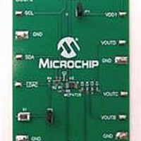
BOARD EVAL 12BIT 4CH DAC MCP4728
Manufacturer
Microchip Technology
Type
D/Ar
Specifications of MCP4728EV
Number Of Dac's
4
Number Of Bits
12
Outputs And Type
1, Single Ended
Data Interface
I²C
Settling Time
6µs
Dac Type
Voltage
Voltage Supply Source
Single
Operating Temperature
-40°C ~ 125°C
Utilized Ic / Part
MCP4728
Product
Data Conversion Development Tools
Resolution
12 bit
Interface Type
I2C
Supply Voltage (max)
5.5 V
Supply Voltage (min)
2.7 V
Silicon Manufacturer
Microchip
Silicon Core Number
MCP4728
Kit Application Type
Data Converter
Application Sub Type
DAC
Kit Contents
Board
For Use With/related Products
MCP4728
Lead Free Status / RoHS Status
Lead free / RoHS Compliant
Lead Free Status / RoHS Status
Lead free / RoHS Compliant, Lead free / RoHS Compliant
Available stocks
Company
Part Number
Manufacturer
Quantity
Price
Company:

Part Number:
MCP4728EV
Manufacturer:
Microchip Technology
Quantity:
135
Company:
Part Number:
MCP4728EV
Manufacturer:
MICROCHIP
Quantity:
12 000


MCP4728
4.5
The device has a precision internal voltage reference
which provides a nominal voltage of 2.048V. The user
can select the internal voltage reference or V
voltage reference source of each channel using the
V
circuit is turned off when all channels select V
their references. However, it stays turned on if any one
of the channels selects the internal reference.
4.6
The LSB is defined as the ideal voltage difference
between two successive codes. LSB sizes of the
MCP4728 device are shown in
TABLE 4-4:
4.7
Each channel has an independent output associated
with its own configuration bit settings and DAC input
code. When the internal voltage reference is selected
(V
to the resistor string DAC of the channel. When the
external reference (V
for the channel’s resistor string DAC.
The V
DAC performance. When the V
voltage reference, any variation or noises on the V
line can directly affect on the DAC output.
The
programmable gain block. The rail-to-rail output
amplifier has a configurable gain of 1 or 2. But the gain
of 2 is not applicable if V
reference. The formula for the analog output voltage is
given in
DS22187A-page 26
Note 1:
REF
(2.048V)
REF
Internal
V
V
V
REF
REF
DD
configuration bit. The internal voltage reference
DD
analog
= internal), it supplies the internal V
Equation 4-1
Voltage Reference
LSB Size
DAC Output Voltage
needs to be as clean as possible for accurate
LSB size varies with the V
When V
G
ignored.
X
Gain (G
Selection
= 1 by default. G
output
x1
x2
x1
LSB SIZES (EXAMPLE)
REF
REF
X
and
)
= V
=V
of
DD
Equation
V
LSB Size
DD
DD
0.5 mV
DD
is selected for the voltage
1 mV
each
, the device uses
) is selected, V
/4096
Table
X
DD
= 2 option is
is selected as the
4-2.
channel
4-4.
DD
2.048V/4096
4.096V/4096
Condition
range.
(Note 1
REF
DD
DD
has
voltage
is used
as the
DD
DD
as
a
4.7.1
The DAC output voltage range varies depending on the
voltage reference selection.
• When the internal reference (V
V
• When the external reference (V
V
EQUATION 4-1:
EQUATION 4-2:
4.8
The following events update the output registers
(V
a.
b.
c.
d.
4.8.1
The user can use the LDAC pin or UDAC bit to upload
the input DAC register to output DAC register (V
However, the UDAC affects only the selected channel
while the LDAC affects all channels. The UDAC bit is
not used in the Fast Mode Writing.
Table 4-5
UDAC bit conditions.
Note that the gain selection bit is not applicable for
V
gain selection bit setting.
Where:
Where:
OUT
OUT
V
selected:
selected:
REF
OUT
REF
D
G
D
LDAC pin to “Low”: Updates all DAC channels.
UDAC bit to “Low”: Updates a selected channel
only.
General Call Software Update Command:
Updates all DAC channels.
Power-On-Reset or General Call Reset com-
mand: Both input and output registers are
updated with EEPROM data. All channels are
affected.
= 0.000V to 4.096V * 4095/4096 for Gain of 2
n
n
x
= 0.000V to 2.048V * 4095/4096 for Gain of 1
= 0.000V to V
):
= V
V
=
=
=
Output Voltage Update
=
OUT
shows the output update vs. LDAC pin and
DD
OUTPUT VOLTAGE RANGE
LDAC PIN AND UDAC BIT
2.048V for internal reference selection
. Gain of 1 is used regardless of the
DAC input code
Gain Setting
DAC input code
=
(
------------------------------ - G
V
V
OUT
REF
DD
4096
V
INTERNAL REFERENCE
V
×
=
© 2009 Microchip Technology Inc.
OUT
OUT
D
(
---------------------------- -
n
V
)
DD
FOR
FOR
4096
×
x
REF
REF
D
V
V
n
REF
REF
)
=2.048V) is
=V
DD
≤
=
=
V
) is
V
DD
DD
OUT
).
Related parts for MCP4728EV
Image
Part Number
Description
Manufacturer
Datasheet
Request
R

Part Number:
Description:
Manufacturer:
Microchip Technology Inc.
Datasheet:
Part Number:
Description:
Manufacturer:
Microchip Technology Inc.
Datasheet:
Part Number:
Description:
Manufacturer:
Microchip Technology Inc.
Datasheet:
Part Number:
Description:
Manufacturer:
Microchip Technology Inc.
Datasheet:
Part Number:
Description:
Manufacturer:
Microchip Technology Inc.
Datasheet:
Part Number:
Description:
Manufacturer:
Microchip Technology Inc.
Datasheet:
Part Number:
Description:
Manufacturer:
Microchip Technology Inc.
Datasheet:
Part Number:
Description:
Manufacturer:
Microchip Technology Inc.
Datasheet: