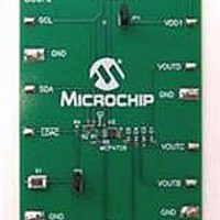
MCP4728EV Microchip Technology, MCP4728EV Datasheet
MCP4728EV
Specifications of MCP4728EV
Available stocks


Related parts for MCP4728EV

MCP4728EV Summary of contents
Page 1
... Microchip Technology Inc. MCP4728 Evaluation Board User’s Guide DS51837A ...
Page 2
... PICDEM, PICDEM.net, PICtail, PIC Select Mode, Total Endurance, TSHARC, WiperLock and ZENA are trademarks of Microchip Technology Incorporated in the U.S.A. and other countries. SQTP is a service mark of Microchip Technology Incorporated in the U.S.A. All other trademarks mentioned herein are property of their respective companies. ...
Page 3
... A.5 Board – Top Pads and Silk .......................................................................... 39 A.6 Board – Bottom Copper Layer ..................................................................... 40 Appendix B. Bill Of Materials (BOM) Appendix C. MCP4728 Read/Write Commands C.1 Introduction .................................................................................................. 43 Worldwide Sales and Service .................................................................................... 46 © 2009 Microchip Technology Inc. MCP4728 EVALUATION BOARD Table of Contents USER’S GUIDE DS51837A-page iii ...
Page 4
... MCP4728 Evaluation Board User’s Guide NOTES: DS51837A-page iv © 2009 Microchip Technology Inc. ...
Page 5
... Appendix B. “Bill Of Materials (BOM)” – lists the parts used to build the MCP4728 Evaluation Board. • Appendix C. “MCP4728 Read/Write Commands” – shows the read/write com- mands for the MCP4728 Evaluation Board. © 2009 Microchip Technology Inc. MCP4728 EVALUATION BOARD Preface NOTICE TO CUSTOMERS TM Serial Analyzer ...
Page 6
... A variable argument; it can be either a type of data (in lowercase characters specific example (in uppercase characters). A menu selection from the menu bar A window or dialog button to click A key on the keyboard Referenced books © 2009 Microchip Technology Inc. Examples #define START c:\autoexec.bat <label>, <exp> MPASMWIN [main.asm] errorlevel {0|1} “ ...
Page 7
... Local sales offices are also available to help customers. A listing of sales offices and locations is included in the back of this document. Technical support is available through the web site at: http://support.microchip.com DOCUMENT REVISION HISTORY Revision A (June 2009) • Initial Release of this Document. © 2009 Microchip Technology Inc. Preface DS51837A-page 3 ...
Page 8
... MCP4728 Evaluation Board User’s Guide NOTES: DS51837A-page 4 © 2009 Microchip Technology Inc. ...
Page 9
... The MCP4728 Evaluation Board has test points for SDL, SDA, and DAC outputs. By connecting an oscilloscope to these I communications through the I V terminals) using a multimeter. Refer to Appendix A. “Schematic and Layouts”. OUT © 2009 Microchip Technology Inc. MCP4728 EVALUATION BOARD TM Serial Analyzer. The following sections cover the topics serial communication signals through the serial communications ...
Page 10
... J1 connector (PICkit Serial Analyzer), then this DD test point monitors the V voltage. You can also connect a new V DD test terminal. Connected to common ground plane of the PC Board SCL pin of the MCP4728 SDA pin of the MCP4728. . (You can disconnect this jumper SS to this DD © 2009 Microchip Technology Inc. ...
Page 11
... A2, A1, A0 Address Bits: Pre-programmed to‘000’. 5. Connecting V Analyzer will provide V LED D1 turns on. 6. Use the PICkit Serial Analyzer PC GUI to send I © 2009 Microchip Technology Inc. Quick Start Instructions from the PICkit Serial Analyzer or use your DD . The JP1 connector selects the V ...
Page 12
... MCP4728 Evaluation Board User’s Guide . USB Cable Connected between the PICkit Serial Analyzer and Personal Computer PICkit Serial Analyzer MCP4728 Evaluation Board FIGURE 1-2: MCP4728 Evaluation Board with the PICkit Serial Analyzer. DS51837A-page 8 Personal Computer DAC Output (Channel B) © 2009 Microchip Technology Inc. ...
Page 13
... Run the PICkit Serial PC Software: It will open to the following GUI. Click the Next button and follow the instructions. FIGURE 1-3: 4. Select the Communication Mode type: I FIGURE 1-4: © 2009 Microchip Technology Inc. Quick Start Instructions PICkit Serial Analyzer Configuration Wizard Welcome Window Master, and click the Next button. ...
Page 14
... Select No on Enable Pull-ups and click the Next button. Note: The MCP4728 Evaluation Board has its own pull-up resistors. FIGURE 1-6: DS51837A-page 10 2 Step Communication Speed Selection bus data rate up to 3.4 MHz, but the Step 3 - Device Pull-Ups Window bus data rate © 2009 Microchip Technology Inc. ...
Page 15
... Case 2: When you use your own V You can also provide your own V test point. In this case, make sure that the JP1 jumper is disconnected. FIGURE 1-7: © 2009 Microchip Technology Inc. Quick Start Instructions voltage of the MCP4728 Evaluation Board and click the Next DD ...
Page 16
... MCP4728 Evaluation Board User’s Guide 8. Click the OK button. You have made all of the PICkit Serial Analyzer Configuration Setups. You are now ready to read/write MCP4728 registers and EEPROM. FIGURE 1-8: DS51837A-page 12 Configuration Wizard - Finishing Step. © 2009 Microchip Technology Inc. ...
Page 17
... Board. The following steps show how to create script files and how to use them. Refer to the PICkit Serial Analyzer User’s Guide (DS51647) for creating the Script file. • Select Communication -----> Script ---> Script Builder FIGURE 1-9: © 2009 Microchip Technology Inc. Quick Start Instructions Creating a Script File with Script Builder. DS51837A-page 13 ...
Page 18
... Detail” are in the exact order as shown here. FIGURE 1-10: Creating a new Script file to select V external selected for all DAC channels. REF REF DD DS51837A-page Scripts” column. = 2.048V). Figure 1-10 shows an REF of each DAC channel. In this example, REF © 2009 Microchip Technology Inc. ...
Page 19
... Serial Analyzer from your computer and recheck the parameter values, including the order of parameters under the “Script Detail” column including the I immediately after sending the I © 2009 Microchip Technology Inc. Quick Start Instructions * * --------> This means there are two bytes to send. ...
Page 20
... The MCP4728 device on the evaluation board has I address bits (A2, A1, A0) = (0,0,0). DS51837A-page 16 of each DAC channel. In this example, Gain REF * * -----> This means there are two bytes to send. -----> Address byte = 1100-0000 (See Note). ---- > Selecting the gain of each channel * (0: Gain gain © 2009 Microchip Technology Inc. ...
Page 21
... Detail” column including the I2C address of the device, and try again until the “Busy” LED turns OFF immediately after sending the I © 2009 Microchip Technology Inc. Quick Start Instructions 2 C Write Command to the 2 C command ...
Page 22
... Make sure the listed parameters in “script Detail” are in the exact order as shown here. FIGURE 1-12: Writing Script File to Write Each DAC Register with a Fast Write Command Using the PICkit Serial Analyzer. DS51837A-page 18 ) when OUT © 2009 Microchip Technology Inc. ...
Page 23
... You can now measure the DAC output voltages (V using a voltmeter. When Examples 1, 2, and 3 are executed sequentially, all channels use an internal reference. Figure 1-13 shows the expectation of each DAC channel out- puts. © 2009 Microchip Technology Inc. Quick Start Instructions * * -------> This means there are nine bytes to send. ...
Page 24
... V = – ----------- - ⎝ ⎠ ⎝ DD 4096 4096 8 4096 Stop 3rd Byte Next DAC Channels ⎞ – LSB ⎠ ⎞ ---------- - – LSB ⎠ ⎞ ----------- - = ---------- - – LSB ⎠ 4096 4 V ⎞ ---------- - – LSB ⎠ and OUT REF DD © 2009 Microchip Technology Inc. ...
Page 25
... Make sure the listed parameters in “script Detail” are in the exact order as shown here. FIGURE 1-14: Writing Script file to Write Channel A for FFFh and Channel B for 800h Using a Multi-write Command. © 2009 Microchip Technology Inc. Quick Start Instructions DS51837A-page 21 ...
Page 26
... Configuration register bits and data nibble -------> Data byte * 2 C address of the device, and try again until the “Busy” LED turns OFF 2 C command. voltage at the V test pins: OUT OUT Write Command to the A and OUT © 2009 Microchip Technology Inc. ...
Page 27
... Input code n LSB = V REF Note that Dn and Gain ( ------------------------------ - OUT Figure 1-15: V for Example 4: Multi-Write Command for Channels A and B with V OUT and Gain = 1. © 2009 Microchip Technology Inc. Quick Start Instructions ) x × ) 4095 ⎛ ⎞ ⎛ 4096 1 – -------------------- - = – ----------- - ⎝ ...
Page 28
... This means there are four bytes to send. -------> Address byte = 1100-0000 (See Note). -------> Command Type and selection of Channel A. -------> Configuration register bits and data nibble for Channel A. -------> Data byte for Channel A (register and its EEPROM © 2009 Microchip Technology Inc. ...
Page 29
... Since the UDAC bit is set to “0” in the command, the device will update the channel output as soon as the command is executed regardless of the condition of the OUT LDAC pin switch S1. © 2009 Microchip Technology Inc. Quick Start Instructions 2 C command. voltage at the V test pins: ...
Page 30
... DD DD 4096 4096 V if external V is selected DD REF 2.048V if internal V is selected. REF Input code V /4096 REF ) must be selected with the following conditions: x × REF n ≤ 4096 ⎞ 1 – ----------- - = V – LSB ⎠ DD 4096 = V and Gain = 1. REF DD © 2009 Microchip Technology Inc. ...
Page 31
... Settings Internal (2.048V), Gain = 1. (c) Channel D Settings: V REF The DAC outputs are updated immediately with the ACK pulse. This example uses the UDAC bit to update the DAC outputs. © 2009 Microchip Technology Inc. Quick Start Instructions = V and Gain = 1. (b) Channel C REF DD = Internal (2 ...
Page 32
... Configuration register bits and data nibble for Ch. D -------> Data byte for Ch address of the device, and try again until the “Busy” LED turns OFF 2 C command. voltage at the V test terminals: OUT OUT Write Command to the B, C, OUT © 2009 Microchip Technology Inc. ...
Page 33
... V Note that Dn and Gain (Gx) must be selected with the following conditions REF ------------------------------ - OUT 4096 FIGURE 1-19: V for Example 6: V OUT © 2009 Microchip Technology Inc. Quick Start Instructions ) Gain ( for Channel B = 0FFF (hex) = 4095 (decimal × ) 4095 ⎛ ⎞ ⎛ 4096 1 – ...
Page 34
... Figure 1-21 for Details in Reading Data. DS51837A-page 30 of the device. If you are using the V DD again and measure the analog voltage ( the same as in Step (b). OUT Read Command ) using a OUT from the PICkit Serial each OUT Reading Data © 2009 Microchip Technology Inc. ...
Page 35
... Ch. D EEPROM: F8-90-FF: FIGURE 1-21: contents: Channel A Register and EEPROM, and Channel B Register and EEPROM, and so on sequentially. See the Read Command and Device Output details in MCP4728 Data Sheet. © 2009 Microchip Technology Inc. Quick Start Instructions DAC B Register DAC A EEPROM DAC C EEPROM ...
Page 36
... The MCP4728 device on the evaluation board has I address bits (A2, A1, A0) = (0,0,0). DS51837A-page -------> This means there are three bytes to send. -------> Address byte = 1100-0000 (See Note). -------> Command Type and Power-Down bits for Chs. A and B. -------> Power-Down bits for Channels C and © 2009 Microchip Technology Inc. ...
Page 37
... I 5. Read the V Once this command is executed, all analog voltage outputs (V the analog output pins (V © 2009 Microchip Technology Inc. Quick Start Instructions 2 C address of the device, and try again until the “Busy” LED turns OFF 2 C command ...
Page 38
... MCP4728 Evaluation Board User’s Guide NOTES: DS51837A-page 34 © 2009 Microchip Technology Inc. ...
Page 39
... Board – Top Silk, Top Pads, and Top Copper Layer • Board – Top Copper and Pads Layer • Board – Top Pads and Silk Layer • Board – Bottom Copper Layer © 2009 Microchip Technology Inc. MCP4728 EVALUATION BOARD USER’S GUIDE DS51837A-page 35 ...
Page 40
... MCP4728 Evaluation Board User’s Guide A.2 BOARD – SCHEMATIC DS51837A-page 36 © 2009 Microchip Technology Inc. ...
Page 41
... A.3 BOARD – TOP SILK, TOP PADS AND TOP COPPER © 2009 Microchip Technology Inc. Schematic and Layouts DS51837A-page 37 ...
Page 42
... MCP4728 Evaluation Board User’s Guide A.4 BOARD – TOP COPPER AND PADS DS51837A-page 38 © 2009 Microchip Technology Inc. ...
Page 43
... A.5 BOARD – TOP PADS AND SILK © 2009 Microchip Technology Inc. Schematic and Layouts DS51837A-page 39 ...
Page 44
... MCP4728 Evaluation Board User’s Guide A.6 BOARD – BOTTOM COPPER LAYER DS51837A-page 40 © 2009 Microchip Technology Inc. ...
Page 45
... SWITCH LIGHT TOUCH 160GF SMD 1 U1 Note 1: The components listed in this Bill of Materials are representative of the PCB assembly. The released BOM used in manufacturing uses all RoHS-compliant components. © 2009 Microchip Technology Inc. MCP4728 EVALUATION BOARD Description Manufacturer ® Panasonic Panasonic - ECG Lite-On Inc ® ...
Page 46
... MCP4728 Evaluation Board User’s Guide NOTES: DS51837A-page 42 © 2009 Microchip Technology Inc. ...
Page 47
... The input and output registers are updated at the acknowledge clock pulse of the last byte. The update does not require LDAC pin or UDAC bit conditions. EEPROM is not affected. © 2009 Microchip Technology Inc. MCP4728 EVALUATION BOARD 2 C address bits are not demonstrated with the This command writes to the DAC input registers sequentially with limited configuration bits ...
Page 48
... LDAC pin or UDAC bit conditions. EEPROM is not affected. DS51837A-page 44 This command writes reference (V ) selection channel. ters This command writes Gain selection bits of each channel. This command writes Power-Down bits of each channel. ters Function ) selection bits of each REF © 2009 Microchip Technology Inc. ...
Page 49
... NOTES: © 2009 Microchip Technology Inc. MCP4728 Read/Write Commands DS51837A-page 45 ...
Page 50
... Fax: 886-3-6578-370 Taiwan - Kaohsiung Tel: 886-7-536-4818 Fax: 886-7-536-4803 Taiwan - Taipei Tel: 886-2-2500-6610 Fax: 886-2-2508-0102 Thailand - Bangkok Tel: 66-2-694-1351 Fax: 66-2-694-1350 © 2009 Microchip Technology Inc. EUROPE Austria - Wels Tel: 43-7242-2244-39 Fax: 43-7242-2244-393 Denmark - Copenhagen Tel: 45-4450-2828 Fax: 45-4485-2829 France - Paris Tel: 33-1-69-53-63-20 ...