MCP4728EV Microchip Technology, MCP4728EV Datasheet - Page 28
MCP4728EV
Manufacturer Part Number
MCP4728EV
Description
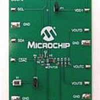
BOARD EVAL 12BIT 4CH DAC MCP4728
Manufacturer
Microchip Technology
Type
D/Ar
Specifications of MCP4728EV
Number Of Dac's
4
Number Of Bits
12
Outputs And Type
1, Single Ended
Data Interface
I²C
Settling Time
6µs
Dac Type
Voltage
Voltage Supply Source
Single
Operating Temperature
-40°C ~ 125°C
Utilized Ic / Part
MCP4728
Product
Data Conversion Development Tools
Resolution
12 bit
Interface Type
I2C
Supply Voltage (max)
5.5 V
Supply Voltage (min)
2.7 V
Silicon Manufacturer
Microchip
Silicon Core Number
MCP4728
Kit Application Type
Data Converter
Application Sub Type
DAC
Kit Contents
Board
For Use With/related Products
MCP4728
Lead Free Status / RoHS Status
Lead free / RoHS Compliant
Lead Free Status / RoHS Status
Lead free / RoHS Compliant, Lead free / RoHS Compliant
Available stocks
Company
Part Number
Manufacturer
Quantity
Price
Company:

Part Number:
MCP4728EV
Manufacturer:
Microchip Technology
Quantity:
135
Company:
Part Number:
MCP4728EV
Manufacturer:
MICROCHIP
Quantity:
12 000


MCP4728
4.10
Each channel has two modes of operation: (a) Normal
mode where analog voltage is available and (b)
Power-Down mode which turns off most of the internal
circuits for power savings.
The user can select the operating mode of each
channel individually by setting the Power-Down
selection bits (PD1 and PD0). For example, the user
can select channel A for normal mode while selecting
all other channels for power-down mode.
See Section 5.6 “Write Commands for DAC Regis-
ters and EEPROM” for more details on the writing the
power-down bits.
Most of the internal circuit in the powered down chan-
nel are turned off. However, the internal voltage refer-
ence circuit is not affected by the Power-Down mode.
The internal voltage reference circuit is turned off only
if all channels select external reference (V
Device actions during Power-Down mode:
• The powered down channel stays in a power sav-
• No analog voltage output at the powered down
• The output (V
• The contents of both the DAC registers and
• Draws less than 40 nA (typical) when all four
Circuits that are not affected during Power-Down
Mode:
• The I
• The internal voltage reference circuit stays
Exiting Power-Down Mode:
The device exits Power-Down mode immediately by
the following commands:
• Any write command for normal mode. Only
• I
• I
DS22187A-page 28
ing condition by turning off most of its circuits.
channel.
channel is switched to a known resistive load. The
value of the resistive load is determined by the
state of the Power-Down bits (PD1 and PD0).
Table 4-7
bit settings.
EEPROM are not changed.
channels are powered down and V
as the voltage reference.
order to receive any command from the Master.
turned-on if it is selected as reference by at least
one channel.
selected channel is affected.
channels are affected.
conditional case. The device exits Power-Down
mode depending on the Power-Down bit settings
in EEPROM as the configuration bits and DAC
input codes are uploaded from EEPROM. All
channels are affected.
2
2
C General Call Reset Command. This is a
C General Call Wake-Up Command. All
2
C serial interface circuits remain active in
Normal and Power-Down Modes
shows the outcome of the Power-Down
OUT
) pin of the powered down
DD
is selected
REF
= V
DD
).
When the DAC operation mode is changed from the
Power-Down to normal mode, there will be a time delay
until the analog output is available. Typical time delay
for the output voltage is approximately 4.5 μs. This time
delay is measured from the acknowledge pulse of the
I
the analog output (V
included in the output settling time specification. See
Section 2.0 “Typical Performance Curves” for more
details.
TABLE 4-7:
FIGURE 4-1:
Power-Down Mode.
2
Note 1:
C serial communication command to the
Resistor String DAC
PD1
0
0
1
1
OP
Amp
In Power-Down mode: V
most of internal circuits in the selected
channel are disabled.
PD0
Control Circuit
Power-Down
0
1
0
1
POWER-DOWN BITS
Normal Mode
1 kΩ resistor to ground (Note 1)
100 kΩ resistor to ground
(Note 1)
500 kΩ resistor to ground
(Note 1)
Output Stage for
OUT
© 2009 Microchip Technology Inc.
Resistive
Load
). This time delay is not
Function
1 kΩ
OUT
is off and
100 kΩ 500 kΩ
beginning
V
OUT
of
Related parts for MCP4728EV
Image
Part Number
Description
Manufacturer
Datasheet
Request
R

Part Number:
Description:
Manufacturer:
Microchip Technology Inc.
Datasheet:
Part Number:
Description:
Manufacturer:
Microchip Technology Inc.
Datasheet:
Part Number:
Description:
Manufacturer:
Microchip Technology Inc.
Datasheet:
Part Number:
Description:
Manufacturer:
Microchip Technology Inc.
Datasheet:
Part Number:
Description:
Manufacturer:
Microchip Technology Inc.
Datasheet:
Part Number:
Description:
Manufacturer:
Microchip Technology Inc.
Datasheet:
Part Number:
Description:
Manufacturer:
Microchip Technology Inc.
Datasheet:
Part Number:
Description:
Manufacturer:
Microchip Technology Inc.
Datasheet: