EVL6566A-75WADP STMicroelectronics, EVL6566A-75WADP Datasheet - Page 36
EVL6566A-75WADP
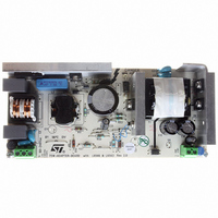
Manufacturer Part Number
EVL6566A-75WADP
Description
BOARD EVAL FOR L6566A
Manufacturer
STMicroelectronics
Type
Power Factor Correctionr
Datasheets
1.L6566ATR.pdf
(51 pages)
2.TSM1014IDT.pdf
(10 pages)
3.L6563ATR.pdf
(39 pages)
4.EVL6566A-75WADP.pdf
(8 pages)
Specifications of EVL6566A-75WADP
Main Purpose
AC/DC, Primary and Secondary Side with PFC
Outputs And Type
1, Isolated
Power - Output
75W
Voltage - Output
19V
Current - Output
4A
Voltage - Input
90 ~ 264VAC
Frequency - Switching
65kHz
Board Type
Fully Populated
Utilized Ic / Part
L6563, L6566A, TSM1014
Input Voltage
90 V to 264 V
Output Voltage
19 V
Dimensions
78 mm x 174 mm
Product
Power Management Modules
Lead Free Status / RoHS Status
Lead free / RoHS Compliant
Regulator Topology
-
Lead Free Status / Rohs Status
Lead free / RoHS Compliant
For Use With/related Products
L6563, L6566A
Other names
497-6449
Available stocks
Company
Part Number
Manufacturer
Quantity
Price


Application information
36/51
Figure 23. OVP function: timing diagram
The ZCD pin will be connected to the auxiliary winding through a resistor divider R
(see
to:
Equation 10
where Vout
number of the secondary winding and Naux the turn number of the auxiliary winding. The
value of R
capability of the internal clamp:
Equation 11
where Vin
winding. See
page 21
To reduce sensitivity to noise and prevent the latch from being erroneously activated, first
the OVP comparator is active only for a small time window (typically, 0.5 µs) starting 2 µs
after MOSFET’s turn-off, to reject the voltage spike associated to the positive-going edges
of the voltage across the auxiliary winding Vaux; second, to stop the L6566A the OVP
comparator must be triggered for four consecutive switching cycles. A counter, which is
reset every time the OVP comparator is not triggered in one switching cycle, is provided to
this purpose.
COUNTER
COUNTER
STATUS
RESET
Vcc_PFC
STROBE
(pin 11)
(pin 6)
(pin 4)
FAULT
COUT
ZCD
GD
Vaux
5V
OVP
Figure 8 on page 20
0
for additional details.
0
Z1
max
NORMAL OPERATION
OVP
will be such that the current sourced by the ZCD pin be within the rated
Section 5.2: Zero current detection and triggering block; oscillator block on
2 µs
is the maximum dc input voltage and Ns the turn number of the primary
is the output voltage value that is to activate the protection, Ns the turn
0
0.5 µs
0
). The divider ratio k
0 → 1
TEMPORARY DISTURBANCE
R
Z
k
1
OVP
≥
1 → 2
3
=
⋅
10
1
Vout
−
2 → 0
3
OVP
5
Naux
OVP
Np
= R
Naux
0
Ns
Vin
Z2
/ (R
max
0 → 1
Z1
FEEDBACK LOOP FAILURE
+ R
Z2
1 → 2
) will be chosen equal
2 → 3
3 → 4
Z1
L6566A
, R
Z2
t
t
t
t
t
t
t
t
t
t
Related parts for EVL6566A-75WADP
Image
Part Number
Description
Manufacturer
Datasheet
Request
R

Part Number:
Description:
BOARD DEMO FOR L6563/LL6566A
Manufacturer:
STMicroelectronics
Datasheet:

Part Number:
Description:
STMicroelectronics [RIPPLE-CARRY BINARY COUNTER/DIVIDERS]
Manufacturer:
STMicroelectronics
Datasheet:
Part Number:
Description:
STMicroelectronics [LIQUID-CRYSTAL DISPLAY DRIVERS]
Manufacturer:
STMicroelectronics
Datasheet:

Part Number:
Description:
BOARD EVAL FOR MEMS SENSORS
Manufacturer:
STMicroelectronics
Datasheet:
Part Number:
Description:
NPN TRANSISTOR POWER MODULE
Manufacturer:
STMicroelectronics
Datasheet:
Part Number:
Description:
TURBOSWITCH ULTRA-FAST HIGH VOLTAGE DIODE
Manufacturer:
STMicroelectronics
Datasheet:
Part Number:
Description:
Manufacturer:
STMicroelectronics
Datasheet:
Part Number:
Description:
DIODE / SCR MODULE
Manufacturer:
STMicroelectronics
Datasheet:
Part Number:
Description:
DIODE / SCR MODULE
Manufacturer:
STMicroelectronics
Datasheet:
Part Number:
Description:
Search -----> STE16N100
Manufacturer:
STMicroelectronics
Datasheet:
Part Number:
Description:
Search ---> STE53NA50
Manufacturer:
STMicroelectronics
Datasheet:
Part Number:
Description:
NPN Transistor Power Module
Manufacturer:
STMicroelectronics
Datasheet: