EVL6566A-75WADP STMicroelectronics, EVL6566A-75WADP Datasheet - Page 21
EVL6566A-75WADP
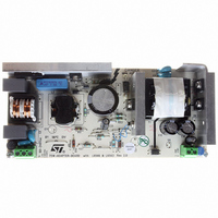
Manufacturer Part Number
EVL6566A-75WADP
Description
BOARD EVAL FOR L6566A
Manufacturer
STMicroelectronics
Type
Power Factor Correctionr
Datasheets
1.L6566ATR.pdf
(51 pages)
2.TSM1014IDT.pdf
(10 pages)
3.L6563ATR.pdf
(39 pages)
4.EVL6566A-75WADP.pdf
(8 pages)
Specifications of EVL6566A-75WADP
Main Purpose
AC/DC, Primary and Secondary Side with PFC
Outputs And Type
1, Isolated
Power - Output
75W
Voltage - Output
19V
Current - Output
4A
Voltage - Input
90 ~ 264VAC
Frequency - Switching
65kHz
Board Type
Fully Populated
Utilized Ic / Part
L6563, L6566A, TSM1014
Input Voltage
90 V to 264 V
Output Voltage
19 V
Dimensions
78 mm x 174 mm
Product
Power Management Modules
Lead Free Status / RoHS Status
Lead free / RoHS Compliant
Regulator Topology
-
Lead Free Status / Rohs Status
Lead free / RoHS Compliant
For Use With/related Products
L6563, L6566A
Other names
497-6449
Available stocks
Company
Part Number
Manufacturer
Quantity
Price


L6566A
5.2
Figure 9.
V
DS
T
ON
T
osc
T
FW
Zero current detection and triggering block; oscillator block
The zero current detection (ZCD) and Triggering blocks switch on the external MOSFET if a
negative-going edge falling below 50 mV is applied to the input (pin 11, ZCD). To do so the
triggering block must be previously armed by a positive-going edge exceeding 100 mV.
This feature is typically used to detect transformer demagnetization for QR operation, where
the signal for the ZCD input is obtained from the transformer’s auxiliary winding used also to
supply the L6566A. The triggering block is blanked for T
turn-off to prevent any negative-going edge that follows leakage inductance
demagnetization from triggering the ZCD circuit erroneously.
The voltage at the pin is both top and bottom limited by a double clamp, as illustrated in the
internal diagram of the ZCD block of
located at 5.7 V, while the lower clamp is located at -0.4 V. The interface between the pin
and the auxiliary winding will be a resistor divider. Its resistance ratio will be properly chosen
(see “
will be such that the current sourced and sunk by the pin be within the rated capability of the
internal clamps (±3 mA).
At converter power-up, when no signal is coming from the ZCD pin, the oscillator starts up
the system. The oscillator is programmed externally by means of a resistor (R
from pin OSC (13) to ground. With good approximation the oscillation frequency f
Equation 2
(with f
at the end of the first oscillator cycle, being zero the voltage on the ZCD pin, the MOSFET
will be turned on, thus starting the first switching cycle right at the beginning of the second
oscillator cycle. At any switching cycle, the MOSFET is turned off as the voltage on the
current sense pin (CS, 7) hits an internal reference set by the line feedforward block, and the
transformer starts demagnetization. If this completes (hence a negative-going edge appears
on the ZCD pin) after a time exceeding one oscillation period T
turn-on, the MOSFET will be turned on again - with some delay to ensure minimum voltage
at turn-on – and the oscillator ramp will be reset. If, instead, the negative-going edge
appears before T
after T
drain ringing cycles will be skipped (“valley-skipping mode”,
frequency will be prevented from exceeding f
Drain ringing cycle skipping as the load is gradually reduced
T
(limit condition)
V
P
in
= P
Section 5.11: OVP block on page 35
osc
osc
in'
in kHz and R
will turn-on the MOSFET and synchronize the oscillator. In this way one or more
osc
t
has elapsed, it will be ignored and only the first negative-going edge
T
V
DS
in kW). As the device is turned on, the oscillator starts immediately;
T
osc
P
in
= P
Figure 8 on page 20
in''
f
osc
< P
”) and the individual resistance values (R
in'
≈
osc
2
R
⋅
.
10
T
3
t
BLANK
. The upper clamp is typically
V
DS
Figure 9
= 2.5 µs after MOSFET’s
osc
T
osc
=1/f
Application information
P
) and the switching
osc
in
= P
from the previous
in'''
< P
T
in''
) connected
osc
Z1
will be:
, R
21/51
Z2
t
)
Related parts for EVL6566A-75WADP
Image
Part Number
Description
Manufacturer
Datasheet
Request
R

Part Number:
Description:
BOARD DEMO FOR L6563/LL6566A
Manufacturer:
STMicroelectronics
Datasheet:

Part Number:
Description:
STMicroelectronics [RIPPLE-CARRY BINARY COUNTER/DIVIDERS]
Manufacturer:
STMicroelectronics
Datasheet:
Part Number:
Description:
STMicroelectronics [LIQUID-CRYSTAL DISPLAY DRIVERS]
Manufacturer:
STMicroelectronics
Datasheet:

Part Number:
Description:
BOARD EVAL FOR MEMS SENSORS
Manufacturer:
STMicroelectronics
Datasheet:
Part Number:
Description:
NPN TRANSISTOR POWER MODULE
Manufacturer:
STMicroelectronics
Datasheet:
Part Number:
Description:
TURBOSWITCH ULTRA-FAST HIGH VOLTAGE DIODE
Manufacturer:
STMicroelectronics
Datasheet:
Part Number:
Description:
Manufacturer:
STMicroelectronics
Datasheet:
Part Number:
Description:
DIODE / SCR MODULE
Manufacturer:
STMicroelectronics
Datasheet:
Part Number:
Description:
DIODE / SCR MODULE
Manufacturer:
STMicroelectronics
Datasheet:
Part Number:
Description:
Search -----> STE16N100
Manufacturer:
STMicroelectronics
Datasheet:
Part Number:
Description:
Search ---> STE53NA50
Manufacturer:
STMicroelectronics
Datasheet:
Part Number:
Description:
NPN Transistor Power Module
Manufacturer:
STMicroelectronics
Datasheet: