RDK-83 Power Integrations, RDK-83 Datasheet - Page 10
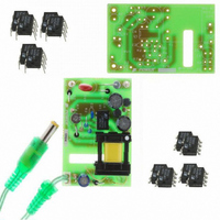
RDK-83
Manufacturer Part Number
RDK-83
Description
KIT DESIGN REF LINKSWITCH LP
Manufacturer
Power Integrations
Series
LinkSwitch®-LPr
Specifications of RDK-83
Main Purpose
AC/DC, Primary Side
Outputs And Type
1, Isolated
Power - Output
1.6W
Voltage - Output
7.7V
Current - Output
210mA
Voltage - Input
85 ~ 265VAC
Regulator Topology
Flyback
Frequency - Switching
66kHz
Board Type
Bare (Unpopulated) and Fully Populated
Utilized Ic / Part
LNK562, LNK563, LNK564
Lead Free Status / RoHS Status
Not applicable / Not applicable
Other names
596-1128


NOTES:
A. In a scheme using a resistor divider network at the FB pin, where R
B. Total current consumption is the sum of I
C Since the output MOSFET is switching, it is diffi cult to isolate the switching current from the supply current at the
D. See Typical Performance Characteristics section Figure 16 for BYPASS pin startup charging waveform.
E. This current is only intended to supply an optional optocoupler connected between the BYPASS and FEEDBACK
F. This parameter is guaranteed by design.
G. This parameter is derived from characterization.
H. Breakdown voltage may be checked against minimum BV
Rev. H 11/08
FEEDBACK Pin
Auto-Restart
Threshold Voltage
Auto-Restart
ON-Time
Auto-Restart
Duty Cycle
10
OUTPUT (cont.)
bias voltage and R
by V
can be used:
To determine the contribution from I
Since I
switching) and the sum of I
DRAIN. An alternative is to measure the BYPASS pin current at 6 V.
pins and not any other external circuitry.
exceeding minimum BV
Parameter
FB
and I
FB
LNK562-564
and V
FB
variations. To determine the contribution from the V
FB
are independent parameters, the composite variation in percent would be
L
is the resistor from the FB pin to the SOURCE pin, the output voltage variation is infl uenced
Symbol
DSS
V
DC
FB(AR)
.
S2
AR
and I
x = 100 #
y = 100 #
DSS
SOURCE = 0 V; T
FB
when FEEDBACK pin is shorted to SOURCE (MOSFET switching).
variation in percent, the following equation can be used:
(Unless Otherwise Specifi ed)
S1
J
K
K
K K
L
J
K
K
K K
L
and I
V
V
V
V
FB(MAX)
FB(TYP)
FB(TYP)
FB(TYP)
Conditions
See Figure 8
V
T
T
DSS
FB
J
J
= 25 °C
= 25 °C
c
= V
c
c
c
when FEEDBACK pin voltage is ≥2 V (MOSFET not
R
R
R
R
J
U
U
U
U
FB(AR)
= -40 to 125 °C
R
R
+ R
R
R
+ R
+ R
+ R
L
L
L
L
DSS
L
L
L
L
m
m
m
by ramping the DRAIN pin voltage up to but not
m
+ I
+ I
+ I
+ I
FB
FB(MAX)
FB(TYP)
FB(TYP)
FB(TYP)
U
variation in percent, the following equation
is the resistor from the FB pin to the rectifi ed
R
R
R
R
U
U
U
U
- 1
- 1
Min
N
O
O
O O
P
N
O
O
O O
P
Typ
100
0.8
12
! x
Max
2
+ y
2
.
Units
ms
%
V
Related parts for RDK-83
Image
Part Number
Description
Manufacturer
Datasheet
Request
R

Part Number:
Description:
KIT REF DESIGN 36-72W MOTOR DRVR
Manufacturer:
Power Integrations
Datasheet:

Part Number:
Description:
KIT REF DESIGN FOR LNK457D
Manufacturer:
Power Integrations
Datasheet:

Part Number:
Description:
REFERENCE DESIGN LINKSWITCH-PH
Manufacturer:
Power Integrations
Datasheet:

Part Number:
Description:
Specifications: Manufacturer: Power Integrations ; Output Voltage: 380 VDC ; Input / Supply Voltage (Max): 264 VAC ; Input / Supply Voltage (Min): 90 VAC ; Mounting Style: Through Hole ; Output Current: 0.913 A ; Output Power: 347 W
Manufacturer:
Power Integrations, Inc.

Part Number:
Description:
KIT REF DESIGN TOP HX FOR TOP258
Manufacturer:
Power Integrations
Datasheet:

Part Number:
Description:
Power Management Modules & Development Tools TOPSwitch-JX REF. DESIGN KIT
Manufacturer:
Power Integrations
Datasheet:
Part Number:
Description:
Power Management IC Development Tools REF DESIGN RDR-292 PFF LED STREET LIGHT
Manufacturer:
Power Integrations

Part Number:
Description:
KIT REF DESIGN FOR LNK403EG
Manufacturer:
Power Integrations
Datasheet:

Part Number:
Description:
KIT REF DESIGN FOR LNK406EG
Manufacturer:
Power Integrations
Datasheet:

Part Number:
Description:
KIT REF DESIGN DG CAPZERO
Manufacturer:
Power Integrations
Datasheet:

Part Number:
Description:
KIT REF DESIGN LINKSWITCH-CV
Manufacturer:
Power Integrations
Datasheet:

Part Number:
Description:
KIT REF DESIGN LINKSWITCH 2
Manufacturer:
Power Integrations
Datasheet:

Part Number:
Description:
KIT REF DESIGN PFS762HG
Manufacturer:
Power Integrations
Datasheet:
Part Number:
Description:
Specifications: Family: Eval Boards - DC/DC & AC/DC (Off-Line) SMPS ; Series: HiperLCS™ ; Main Purpose: DC/DC, Step Down ; Outputs and Type: 1, Isolated ; Power - Output: 150W ; Voltage - Output: 24V ; Current - Output: 6.25A ; Voltage - Input:
Manufacturer:
Power Integrations, Inc.
Datasheet:

Part Number:
Description:
KIT REF DESIGN 1.2W PS TN FAMILY
Manufacturer:
Power Integrations
Datasheet: