MULTIPHSPOL-RD Silicon Laboratories Inc, MULTIPHSPOL-RD Datasheet - Page 7
MULTIPHSPOL-RD
Manufacturer Part Number
MULTIPHSPOL-RD
Description
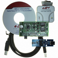
KIT REFERENCE DESIGN FOR SI825X
Manufacturer
Silicon Laboratories Inc
Type
Other Power Managementr
Specifications of MULTIPHSPOL-RD
Main Purpose
DC/DC, Step Down
Outputs And Type
1, Non-Isolated
Voltage - Output
3.3V
Current - Output
40A
Voltage - Input
10 ~ 15V
Regulator Topology
Buck
Frequency - Switching
391kHz
Board Type
Fully Populated
Utilized Ic / Part
SI8250, SI8251, SI8252
Input Voltage
10 V to 15 V
Output Voltage
3.3 V
Interface Type
USB
Product
Power Management Modules
Supply Current
10 A
For Use With/related Products
Si8250
Lead Free Status / RoHS Status
Contains lead / RoHS non-compliant
Power - Output
-
Lead Free Status / Rohs Status
Lead free / RoHS Compliant
Other names
336-1323


Table 5. ADC1 Specifications
TA = –40 to +125 °C, V
Table 6. DSP Filter Engine Electrical Specifications
T
Sampling frequency
Resolution
LSB size
Differential input voltage range
Common-mode input voltage range
Integral nonlinearity
Differential nonlinearity
Gain error
Offset error
Input bias current
Standby mode supply current
Operating mode supply current
*Note: LSB size (mV) is programmable using the RES[3:0] bits in the ADC1CN register.
Resolution
Dithering
Standby mode supply current
Notes:
A
= –40 to +125 °C, V
1. Internal word length = 22 bits.
2. Up to a total 15 bits of resolution when dithering is enabled.
2
1
Parameter
Parameter
DD
DD
= 2.5 V, SYSCLK = 25 MHz, PLLCLK = 200 MHz unless otherwise specified.
= 2.5 V, SYSCLK = 25 MHz, PLLCLK = 200 MHz unless otherwise specified.
Conditions
ADCSP1 = 0
ADCSP2 = 0
ADCSP1 = 1
ADCSP2 = 0
ADCSP1 = 0
ADCSP2 = 1
ADCSP1 = 1
ADCSP2 = 1
Conditions
Disabled
Disabled
*
Rev. 1.0
Min
–32
0.8
Min
–2
–1
—
—
—
—
—
—
—
—
—
—
4
—
—
—
1.25
Typ
2.5
0.1
10
—
—
—
—
—
—
—
5
5
3
5
Typ
0.1
—
—
Si8250/1/2
Max
+31
1.3
20
+2
+1
—
—
—
—
—
—
—
—
6
3
Max
—
9
6
Units
Msps
LSB
LSB
LSB
Bits
mV
mV
mA
Units
µA
µA
%
V
Bits
Bits
µA
7
Related parts for MULTIPHSPOL-RD
Image
Part Number
Description
Manufacturer
Datasheet
Request
R

Part Number:
Description:
SMD/C°/SINGLE-ENDED OUTPUT SILICON OSCILLATOR
Manufacturer:
Silicon Laboratories Inc
Part Number:
Description:
Manufacturer:
Silicon Laboratories Inc
Datasheet:
Part Number:
Description:
N/A N/A/SI4010 AES KEYFOB DEMO WITH LCD RX
Manufacturer:
Silicon Laboratories Inc
Datasheet:
Part Number:
Description:
N/A N/A/SI4010 SIMPLIFIED KEY FOB DEMO WITH LED RX
Manufacturer:
Silicon Laboratories Inc
Datasheet:
Part Number:
Description:
N/A/-40 TO 85 OC/EZLINK MODULE; F930/4432 HIGH BAND (REV E/B1)
Manufacturer:
Silicon Laboratories Inc
Part Number:
Description:
EZLink Module; F930/4432 Low Band (rev e/B1)
Manufacturer:
Silicon Laboratories Inc
Part Number:
Description:
I°/4460 10 DBM RADIO TEST CARD 434 MHZ
Manufacturer:
Silicon Laboratories Inc
Part Number:
Description:
I°/4461 14 DBM RADIO TEST CARD 868 MHZ
Manufacturer:
Silicon Laboratories Inc
Part Number:
Description:
I°/4463 20 DBM RFSWITCH RADIO TEST CARD 460 MHZ
Manufacturer:
Silicon Laboratories Inc
Part Number:
Description:
I°/4463 20 DBM RADIO TEST CARD 868 MHZ
Manufacturer:
Silicon Laboratories Inc
Part Number:
Description:
I°/4463 27 DBM RADIO TEST CARD 868 MHZ
Manufacturer:
Silicon Laboratories Inc
Part Number:
Description:
I°/4463 SKYWORKS 30 DBM RADIO TEST CARD 915 MHZ
Manufacturer:
Silicon Laboratories Inc
Part Number:
Description:
N/A N/A/-40 TO 85 OC/4463 RFMD 30 DBM RADIO TEST CARD 915 MHZ
Manufacturer:
Silicon Laboratories Inc
Part Number:
Description:
I°/4463 20 DBM RADIO TEST CARD 169 MHZ
Manufacturer:
Silicon Laboratories Inc