MULTIPHSPOL-RD Silicon Laboratories Inc, MULTIPHSPOL-RD Datasheet - Page 16
MULTIPHSPOL-RD
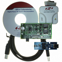
Manufacturer Part Number
MULTIPHSPOL-RD
Description
KIT REFERENCE DESIGN FOR SI825X
Manufacturer
Silicon Laboratories Inc
Type
Other Power Managementr
Specifications of MULTIPHSPOL-RD
Main Purpose
DC/DC, Step Down
Outputs And Type
1, Non-Isolated
Voltage - Output
3.3V
Current - Output
40A
Voltage - Input
10 ~ 15V
Regulator Topology
Buck
Frequency - Switching
391kHz
Board Type
Fully Populated
Utilized Ic / Part
SI8250, SI8251, SI8252
Input Voltage
10 V to 15 V
Output Voltage
3.3 V
Interface Type
USB
Product
Power Management Modules
Supply Current
10 A
For Use With/related Products
Si8250
Lead Free Status / RoHS Status
Contains lead / RoHS non-compliant
Power - Output
-
Lead Free Status / Rohs Status
Lead free / RoHS Compliant
Other names
336-1323


Si8250/1/2
3.1. System Operation
Figure 2 shows the Si8250/1/2 controlling a non-
isolated dc/dc converter operating in digital voltage
mode control. The output voltage signal connects to the
V
common-mode voltage range applied to ADC1 to a
maximum of V
divider and the capacitor form an anti-aliasing filter with
a cutoff frequency equal to ADC1 sampling frequency
divided by 2 (the amplitudes of frequencies above fS/2
must be minimized to prevent aliasing).
Differential ADC1 and the DSP Filter Engine together
perform the same function as an analog error amplifier
and associated RC compensation network. ADC1
digitizes the difference between the scaled output
voltage and a programmable reference voltage provided
by the REFDAC. The ADC1 output signal is frequency-
compensated (in the digital domain) by the DSP Filter
Engine. The resulting output from the DSP Filter Engine
is a digital code that represents the compensated duty
cycle ratio, u(n). The digital PWM generator (DPWM)
directly varies output timing to the external gate drivers
based on the value of u(n) until the difference between
V
Sensing circuitry within the power stages (current
transformer, sense amp, etc.) provides a signal
representative of inductor or transformer current. This
signal connects to the pulse-by-pulse current-limiting
hardware in the Si8250/1/2 via the IPK input pin. This
current-limiting circuitry is similar to that found in a
voltage mode analog PWM. It contains a fast analog
comparator and a programmable leading-edge blanking
circuit to prevent unwanted tripping of the current-
sensing circuitry on the leading edge of the current
pulse. Current limiting occurs when the sensed current
exceeds the programmed threshold. When this occurs,
the ongoing active portions of the PWM outputs are
terminated. A programmable OCP counter keeps track
of the number of consecutive current limit cycles and
automatically shuts the supply down when the
accumulated number of limit cycles exceeds the
programmed maximum.
The System Management Processor is based on a 50
million instruction per second (MIPS) 8051 CPU and
dedicated A/D converter (ADC0). ADC0 digitizes key
analog parameters that are used by the MCU to provide
protection and manage and control other aspects of the
power system. Onboard digital peripherals include
timers, an SMBus interface port, and a universal
asynchronous receiver/transmitter (UART) for serial
communications (useful for communicating across an
isolation boundary).
16
SENSE
SENSE
and the ADC1 reference level is driven to zero.
input through a resistive divider, limiting the
REF
. The equivalent resistance of the
Rev. 1.0
The System Management Processor serves several
purposes:
1. Continuously optimizes Control Processor operation
2. Executes user-specific algorithms (e.g. support for
3. Provides regulation for low-bandwidth system
4. Performs system fault detection and recovery
5. Provides system housekeeping functions, such as
6. Manages external device functions (e.g. external
Si8250/1/2 system development requires using the
Si8250DK, a comprehensive development kit providing
all required hardware and software for control system
design. It comes complete with prewritten and verified
application software and a set of tools that enable the
user to adapt this software to the end application. It also
includes a turnkey isolated half-bridge dc/dc converter
based
experimentation.
3.2. Control Processor Functional Block
3.2.1. ADC 1
Differential input, 10 Msps control loop analog-to-digital
converter. ADC1 digitizes the difference between the
V
level from the REFDAC. ADC1 can be operated at 1.25,
2.5, 5, or 10 Msps and has a programmable LSB size to
prevent limit cycle oscillation (Limit cycle oscillation can
also be avoided using dithering to increase DPWM
resolution). ADC1 has programmable conversion rates
of 1.25, 2.5, 5, or 10 Msps to accommodate a wide loop
gain range. ADC1 also contains a hardware transient
detector that interrupts the CPU at the onset of an
output load or unload transient. The CPU responds by
executing specific algorithms to accelerate output
recovery. These algorithms may include increasing loop
bandwidth or other measures.
3.2.2. REFDAC
9-bit digital-to-analog converter provides the output
voltage reference setting. The REFDAC uses the
onboard band gap as its voltage reference, or it can be
referenced to an external voltage reference source.
REFDAC is used for output voltage calibration,
margining, and positioning. The CPU continuously
manages the REFDAC during soft-start and soft-stop.
3.2.3. DSP Filter Engine
This two-stage loop compensation filter is the functional
equivalent of an active RC compensation in an analog
SENSE
(e.g. efficient optimization)
proprietary system interfaces)
variables (e.g. V
SMBus communication support
supply sequencing, fan control/monitoring)
Descriptions (Figure 1)
input and the programmable voltage reference
on
the
IN
Si8250/1/2
feed-forward)
for
evaluation
and
Related parts for MULTIPHSPOL-RD
Image
Part Number
Description
Manufacturer
Datasheet
Request
R

Part Number:
Description:
SMD/C°/SINGLE-ENDED OUTPUT SILICON OSCILLATOR
Manufacturer:
Silicon Laboratories Inc
Part Number:
Description:
Manufacturer:
Silicon Laboratories Inc
Datasheet:
Part Number:
Description:
N/A N/A/SI4010 AES KEYFOB DEMO WITH LCD RX
Manufacturer:
Silicon Laboratories Inc
Datasheet:
Part Number:
Description:
N/A N/A/SI4010 SIMPLIFIED KEY FOB DEMO WITH LED RX
Manufacturer:
Silicon Laboratories Inc
Datasheet:
Part Number:
Description:
N/A/-40 TO 85 OC/EZLINK MODULE; F930/4432 HIGH BAND (REV E/B1)
Manufacturer:
Silicon Laboratories Inc
Part Number:
Description:
EZLink Module; F930/4432 Low Band (rev e/B1)
Manufacturer:
Silicon Laboratories Inc
Part Number:
Description:
I°/4460 10 DBM RADIO TEST CARD 434 MHZ
Manufacturer:
Silicon Laboratories Inc
Part Number:
Description:
I°/4461 14 DBM RADIO TEST CARD 868 MHZ
Manufacturer:
Silicon Laboratories Inc
Part Number:
Description:
I°/4463 20 DBM RFSWITCH RADIO TEST CARD 460 MHZ
Manufacturer:
Silicon Laboratories Inc
Part Number:
Description:
I°/4463 20 DBM RADIO TEST CARD 868 MHZ
Manufacturer:
Silicon Laboratories Inc
Part Number:
Description:
I°/4463 27 DBM RADIO TEST CARD 868 MHZ
Manufacturer:
Silicon Laboratories Inc
Part Number:
Description:
I°/4463 SKYWORKS 30 DBM RADIO TEST CARD 915 MHZ
Manufacturer:
Silicon Laboratories Inc
Part Number:
Description:
N/A N/A/-40 TO 85 OC/4463 RFMD 30 DBM RADIO TEST CARD 915 MHZ
Manufacturer:
Silicon Laboratories Inc
Part Number:
Description:
I°/4463 20 DBM RADIO TEST CARD 169 MHZ
Manufacturer:
Silicon Laboratories Inc