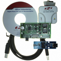
MULTIPHSPOL-RD Silicon Laboratories Inc, MULTIPHSPOL-RD Datasheet - Page 21

MULTIPHSPOL-RD
Manufacturer Part Number
MULTIPHSPOL-RD
Description
KIT REFERENCE DESIGN FOR SI825X
Manufacturer
Silicon Laboratories Inc
Type
Other Power Managementr
Specifications of MULTIPHSPOL-RD
Main Purpose
DC/DC, Step Down
Outputs And Type
1, Non-Isolated
Voltage - Output
3.3V
Current - Output
40A
Voltage - Input
10 ~ 15V
Regulator Topology
Buck
Frequency - Switching
391kHz
Board Type
Fully Populated
Utilized Ic / Part
SI8250, SI8251, SI8252
Input Voltage
10 V to 15 V
Output Voltage
3.3 V
Interface Type
USB
Product
Power Management Modules
Supply Current
10 A
For Use With/related Products
Si8250
Lead Free Status / RoHS Status
Contains lead / RoHS non-compliant
Power - Output
-
Lead Free Status / Rohs Status
Lead free / RoHS Compliant
Other names
336-1323
6. Layout Considerations
The mixed-signal nature of the Si8250/1/2 mandates
clean bias supplies and ground returns. It is best to
provide separate ground planes for analog, digital, and
power switch returns. These planes should tie together
at only one point to eliminate the possibility of circulating
ground currents. For best performance, the V
should be decoupled from the main supply. The LQFP-
32 package provides the best noise performance
because it has separate analog and digital V
ground inputs (V
lengths as short
10 uF
as possible
Keep trace
DDA
lengths as short
10 uF
as possible
Keep trace
, GNDA).
GNDA
0.1 uF
Figure 10. Power Supply Connections for LQFP-32 Package
Figure 11. Power Supply Connections for QFN-28 Package
0.1 uF
GNDA
V
500 mA, 40 Ω
Si8250/1/2
Ferrite bead
DDA
DD
DD
supply
GND
VDD
V
GND
500 mA, 40 Ω
and
Ferrite bead
DD
Rev. 1.0
Si8250/1/2
As shown in Figure 10, the V
consisting of a 1 Ω resistor in series with a 500 mA,
40 Ω ferrite bead and a parallel combination of a 10 µF
with a 0.1 µF high-frequency bypass capacitor. All
connections should be kept as short as possible. V
and GNDA should be connected into their respective
ground planes. The QFN-28 package shares analog
and digital power with ground on the same pins. Power
supply decoupling is shown in Figure 11. Again, all
connections should be kept as short as possible.
10 uF
1 Ω
0.1 uF
1 Ω
DDA
Si8250/1/2
2.5 V
is decoupled by a filter
2.5 V
DDA
21


