STEVAL-CBL006V1 STMicroelectronics, STEVAL-CBL006V1 Datasheet - Page 18
STEVAL-CBL006V1
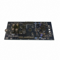
Manufacturer Part Number
STEVAL-CBL006V1
Description
DEMO BOARD BASED ON LNBH24
Manufacturer
STMicroelectronics
Type
DC/DC Switching Converters, Regulators & Controllersr
Specifications of STEVAL-CBL006V1
Main Purpose
Special Purpose DC/DC, LNB
Outputs And Type
2, Non-Isolated
Voltage - Input
8 ~ 15V
Regulator Topology
Boost
Board Type
Fully Populated
Utilized Ic / Part
LNBH24
Input Voltage
12 V
Interface Type
I2C
Product
Power Management Modules
Supply Current
500 mA
Silicon Manufacturer
ST Micro
Silicon Core Number
LNBH24
Kit Application Type
Power Management
Application Sub Type
LNB Power Supply
Kit Contents
Board
Lead Free Status / RoHS Status
Lead free / RoHS Compliant
Current - Output
-
Voltage - Output
-
Power - Output
-
Frequency - Switching
-
Lead Free Status / Rohs Status
Lead free / RoHS Compliant
For Use With/related Products
LNBH24
Other names
497-8718


Table 7.
Note:
7.5
7.6
7.7
18/30
IMON
0/1
VMON
0/1
Register
Values are typical unless otherwise specified.
Power-on I²C interface reset
The I²C interface built in the LNBH24 is automatically reset at power-ON. As long as the V
stays below the undervoltage lockout (UVL) threshold (6.7 V), the interface will not respond
to any I²C command and the system registers (SR) are initialized to all zeroes, thus keeping
the power blocks disabled. Once the V
operative and the SRs can be configured by the main MCU. This is due to 500 mV
hysteresis provided in the UVL threshold to avoid false re-triggering of the power-ON reset
circuit.
Address pin
For each section of the LNBH24 it is possible to select two I²C interface addresses by
means of the relevant ADDR pin. The ADDR pins are TTL-compatible and can be set as per
address pins characteristics
DiSEqC™ implementation for each section A/B
LNBH24 helps system designer to implement the bi-directional DiSEqC 2.0 protocol by
allowing easy PWK modulation/demodulation of the 22 kHz carrier. Between the LNBH24
and the main MCU the PWK data is exchanged using logic levels that are compatible with
both 3.3 V and 5 V MCU. This data exchange is made through two dedicated pins, DSQIN
and DSQOUT, in order to maintain the timing relationships between the PWK data and the
PWK modulation as accurate as possible. These two pins should be directly connected to
two I/O pins of the MCU, thus leaving to the firmware the task of encoding and decoding the
PWK data in accordance with the DiSEqC protocol. Full compliance of the system to the
specification is thus not implied by the bare use of the LNBH24. The system designer should
also take in consideration the bus hardware requirements, which can be simply
accomplished by the R-L termination connected on the V
in the typical application circuits in
during the tone transmission, LNBH24 has dedicated Tone output (V
after the filter and must be enabled by setting the TTX function to HIGH only during the tone
transmission (see DiSEqC 2.0 implementation in sections
DiSEqC 1.x and non-DiSEqC system need this termination connected through a bypass
capacitor and after an R-L filter with 15 Ω in parallel with a 220 µH-270 µH inductor.
However, there is no need for tone decoding, so the DETIN and DSQOUT pins can be left
connected to GND.
TMON
0/1
LLC
exactly the same as
These bits are read
last write operation
they were left after
VSEL
Table
EN
10.
Figure
OTF
0
1
CC
rises above 7.3 V typ. The I²C interface becomes
4. To avoid any losses due to the R-L impedance
OLF
0
1
T
T
I
I
These bits are set to 1 if the relative parameter
is out of the specification limits.
O
O
J
J
< I
> I
< 135°C, normal operation
> 150°C, power blocks disabled
OMAX
OMAX
OUT
, normal operation
, Overload Protection triggered
2.2
pins of the LNBH24, as shown
and 2.3). Also unidirectional
Function
oTX
) that is connected
CC
Related parts for STEVAL-CBL006V1
Image
Part Number
Description
Manufacturer
Datasheet
Request
R

Part Number:
Description:
BOARD EVAL FOR MEMS SENSORS
Manufacturer:
STMicroelectronics
Datasheet:

Part Number:
Description:
KIT DEV STARTER ST10F276Z5
Manufacturer:
STMicroelectronics
Datasheet:

Part Number:
Description:
BOARD EVAL UPS 450W VOUT=220V
Manufacturer:
STMicroelectronics
Datasheet:

Part Number:
Description:
BOARD STLM75/STDS75/ST72F651
Manufacturer:
STMicroelectronics
Datasheet:

Part Number:
Description:
EVAL BOARD ENERGY METER MONO
Manufacturer:
STMicroelectronics
Datasheet:

Part Number:
Description:
EVAL BOARD ENERGY METER MONO
Manufacturer:
STMicroelectronics
Datasheet:

Part Number:
Description:
EVAL BOARD ENERGY METER MONO
Manufacturer:
STMicroelectronics
Datasheet:

Part Number:
Description:
BOARD EVAL BASED ON TS2012IQT
Manufacturer:
STMicroelectronics
Datasheet:

Part Number:
Description:
BOARD EVAL FOR TS4962MEIJT
Manufacturer:
STMicroelectronics
Datasheet:

Part Number:
Description:
BOARD DEMO ACCELEROMETER DIL24
Manufacturer:
STMicroelectronics
Datasheet:

Part Number:
Description:
STMicroelectronics [RIPPLE-CARRY BINARY COUNTER/DIVIDERS]
Manufacturer:
STMicroelectronics
Datasheet:
Part Number:
Description:
STMicroelectronics [LIQUID-CRYSTAL DISPLAY DRIVERS]
Manufacturer:
STMicroelectronics
Datasheet:
Part Number:
Description:
BOARD EVAL FOR MEMS SENSORS
Manufacturer:
STMicroelectronics
Datasheet: