STEVAL-CBL006V1 STMicroelectronics, STEVAL-CBL006V1 Datasheet - Page 14
STEVAL-CBL006V1
Manufacturer Part Number
STEVAL-CBL006V1
Description
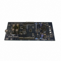
DEMO BOARD BASED ON LNBH24
Manufacturer
STMicroelectronics
Type
DC/DC Switching Converters, Regulators & Controllersr
Specifications of STEVAL-CBL006V1
Main Purpose
Special Purpose DC/DC, LNB
Outputs And Type
2, Non-Isolated
Voltage - Input
8 ~ 15V
Regulator Topology
Boost
Board Type
Fully Populated
Utilized Ic / Part
LNBH24
Input Voltage
12 V
Interface Type
I2C
Product
Power Management Modules
Supply Current
500 mA
Silicon Manufacturer
ST Micro
Silicon Core Number
LNBH24
Kit Application Type
Power Management
Application Sub Type
LNB Power Supply
Kit Contents
Board
Lead Free Status / RoHS Status
Lead free / RoHS Compliant
Current - Output
-
Voltage - Output
-
Power - Output
-
Frequency - Switching
-
Lead Free Status / Rohs Status
Lead free / RoHS Compliant
For Use With/related Products
LNBH24
Other names
497-8718


6
6.1
6.2
6.3
6.4
6.5
14/30
I²C bus interface
Data transmission from main MCU to the LNBH24 and vice-versa takes place through the 2
wires I²C bus Interface, consisting of the 2 SDA and SCL lines (pull-up resistors to positive
supply voltage must be externally connected).
Data validity
As shown in
the clock. The HIGH and LOW state of the data line can only change when the clock signal
on the SCL line is LOW.
Start and stop condition
As shown in
SCL is HIGH. The stop condition is a LOW to HIGH transition of the SDA line while SCL is
HIGH. A STOP condition must be sent before each START condition.
Byte format
Every byte transferred to the SDA line must contain 8 bits. Each byte must be followed by an
acknowledge bit. The MSB is transferred first.
Acknowledge
The master (MCU) puts a resistive HIGH level on the SDA line during the acknowledge clock
pulse (see
the SDA line during the acknowledge clock pulse, so that the SDA line is stable LOW during
this clock pulse. The peripheral which has been addressed has to generate acknowledge
after the reception of each byte, otherwise the SDA line remains at the HIGH level during the
ninth clock pulse time. In this case the master transmitter can generate the STOP
information in order to abort the transfer. The LNBH24 will not generate acknowledge if the
V
Transmission without acknowledge
Avoiding to detect the acknowledges of the LNBH24, the MCU can use a simpler
transmission: simply it waits one clock without checking the slave acknowledging, and sends
the new data. This approach of course is less protected from malfunctions and decreases
the noise immunity.
CC
supply is below the under-voltage lockout threshold (6.7 V typ.).
Figure
Figure 5
Figure 6
7). The peripheral (LNBH24) that acknowledges has to pull-down (LOW)
the data on the SDA line must be stable during the high semi-period of
a start condition is a HIGH to LOW transition of the SDA line while
Related parts for STEVAL-CBL006V1
Image
Part Number
Description
Manufacturer
Datasheet
Request
R

Part Number:
Description:
BOARD EVAL FOR MEMS SENSORS
Manufacturer:
STMicroelectronics
Datasheet:

Part Number:
Description:
KIT DEV STARTER ST10F276Z5
Manufacturer:
STMicroelectronics
Datasheet:

Part Number:
Description:
BOARD EVAL UPS 450W VOUT=220V
Manufacturer:
STMicroelectronics
Datasheet:

Part Number:
Description:
BOARD STLM75/STDS75/ST72F651
Manufacturer:
STMicroelectronics
Datasheet:

Part Number:
Description:
EVAL BOARD ENERGY METER MONO
Manufacturer:
STMicroelectronics
Datasheet:

Part Number:
Description:
EVAL BOARD ENERGY METER MONO
Manufacturer:
STMicroelectronics
Datasheet:

Part Number:
Description:
EVAL BOARD ENERGY METER MONO
Manufacturer:
STMicroelectronics
Datasheet:

Part Number:
Description:
BOARD EVAL BASED ON TS2012IQT
Manufacturer:
STMicroelectronics
Datasheet:

Part Number:
Description:
BOARD EVAL FOR TS4962MEIJT
Manufacturer:
STMicroelectronics
Datasheet:

Part Number:
Description:
BOARD DEMO ACCELEROMETER DIL24
Manufacturer:
STMicroelectronics
Datasheet:

Part Number:
Description:
STMicroelectronics [RIPPLE-CARRY BINARY COUNTER/DIVIDERS]
Manufacturer:
STMicroelectronics
Datasheet:
Part Number:
Description:
STMicroelectronics [LIQUID-CRYSTAL DISPLAY DRIVERS]
Manufacturer:
STMicroelectronics
Datasheet:
Part Number:
Description:
BOARD EVAL FOR MEMS SENSORS
Manufacturer:
STMicroelectronics
Datasheet: