EVAL-AD7708EBZ Analog Devices Inc, EVAL-AD7708EBZ Datasheet - Page 9
EVAL-AD7708EBZ
Manufacturer Part Number
EVAL-AD7708EBZ
Description
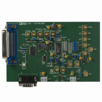
BOARD EVAL FOR AD7708
Manufacturer
Analog Devices Inc
Specifications of EVAL-AD7708EBZ
Number Of Adc's
1
Number Of Bits
16
Sampling Rate (per Second)
1.37k
Data Interface
Serial
Inputs Per Adc
8 Single or 4 Differential
Input Range
±2.5 V
Power (typ) @ Conditions
3.84mW @ 3 V
Voltage Supply Source
Analog and Digital
Operating Temperature
-40°C ~ 85°C
Utilized Ic / Part
AD7708
Lead Free Status / RoHS Status
Lead free / RoHS Compliant
Other names
EVAL-AD7708EB
EVAL-AD7708EB
EVAL-AD7708EB


TIMING CHARACTERISTICS
DGND = 0 V; XTAL = 32.768 kHz; Input Logic 0 = 0 V, Logic 1 = DV
Parameter
t
t
Read Operation
Write Operation
NOTES
1
2
3
4
5
6
7
Specifications subject to change without notice.
1
2
Sample tested during initial release to ensure compliance. All input signals are specified with tr = tf = 5 ns (10% to 90% of DV
level of 1.6 V.
See Figures 1 and 2.
SCLK active edge is falling edge of SCLK.
These numbers are measured with the load circuit of Figure 1 and defined as the time required for the output to cross the V
This specification only comes into play if CS goes low while SCLK is low. It is required primarily for interfacing to DSP machines.
These numbers are derived from the measured time taken by the data output to change 0.5 V when loaded with the load circuit of Figure 1. The measured number is
then extrapolated back to remove effects of charging or discharging the 50 pF capacitor. This means that the times quoted in the timing characteristics are the true
bus relinquish times of the part and as such are independent of external bus loading capacitances.
RDY returns high after the first read from the device after an output update. The same data can be read again, if required, while RDY is high, although care should
be taken that subsequent reads do not occur close to the next output update.
t
t
t
t
t
t
t
t
t
t
t
t
t
t
t
3
4
5
5A
6
7
8
9
10
11
12
13
14
15
16
4
6
4, 5
Limit at T
(B Version)
32.768
50
0
0
0
60
80
0
60
80
100
100
0
10
80
100
0
30
25
100
100
0
1, 2
MIN
TO OUTPUT
, T
(AV
MAX
DD
PIN
= 2.7 V to 3.6 V or AV
50pF
Unit
kHz typ
ns min
ns min
ns min
ns min
ns max
ns max
ns min
ns max
ns max
ns min
ns min
ns min
ns min
ns max
ns max
ns min
ns min
ns min
ns min
ns min
ns min
DD
unless otherwise noted.
I
I
(200 A WITH DV
100 A WITH DV
SINK
SOURCE
DD
100 A WITH DV
(1.6mA WITH DV
= 5 V
1.6V
Conditions/Comments
Crystal Oscillator Frequency
RESET Pulsewidth
RDY to CS Setup Time
CS Falling Edge to SCLK Active Edge Setup Time
SCLK Active Edge to Data Valid Delay
DV
DV
CS Falling Edge to Data Valid Delay
DV
DV
SCLK High Pulsewidth
SCLK Low Pulsewidth
CS Rising Edge to SCLK Inactive Edge Hold Time
Bus Relinquish Time after SCLK Inactive Edge
SCLK Active Edge to RDY High
CS Falling Edge to SCLK Active Edge Setup Time
Data Valid to SCLK Edge Setup Time
Data Valid to SCLK Edge Hold Time
SCLK High Pulsewidth
SCLK Low Pulsewidth
CS Rising Edge to SCLK Edge Hold Time
DD
DD
5%; DV
= 3V)
DD
DD
DD
DD
= 5V
DD
DD
= 4.5 V to 5.5 V
= 2.7 V to 3.6 V
= 4.5 V to 5.5 V
= 2.7 V to 3.6 V
= 3V)
= 5V
DD
= 2.7 V to 3.6 V or DV
OL
or V
DD
AD7708/AD7718
) and timed from a voltage
OH
limits.
DD
= 5 V
3, 7
3
3
5%; AGND =
3
3
3
3
Related parts for EVAL-AD7708EBZ
Image
Part Number
Description
Manufacturer
Datasheet
Request
R


Part Number:
Description:
BOARD EVAL FOR SI270X-A
Manufacturer:
Silicon Laboratories Inc
Datasheet:

Part Number:
Description:
BUCK CONV REF DESIGN KIT IP1201
Manufacturer:
International Rectifier
Datasheet:
Part Number:
Description:
BOARD DEMO SYNC DUAL BUCK CNVTER
Manufacturer:
International Rectifier
Datasheet:
Part Number:
Description:
BOARD DEMO SYNC BUCK CONVETER
Manufacturer:
International Rectifier
Datasheet:

Part Number:
Description:
EVALBOARD/EB Omnidirectional microphone - Analog
Manufacturer:
Analog Devices
Datasheet:
Part Number:
Description:
EVALBOARD/EB Omnidirectional microphone - Analog
Manufacturer:
Analog Devices
Datasheet:


Part Number:
Description:
BOARD EVAL LED DRIVER LT3756
Manufacturer:
Linear Technology
Datasheet:

Part Number:
Description:
BOARD EVAL FOR AD7741/7742
Manufacturer:
Analog Devices Inc
Datasheet:

Part Number:
Description:
±1.7g Dual-Axis IMEMS Accelerometer Evaluation Board
Manufacturer:
Analog Devices Inc
Datasheet:

Part Number:
Description:
IC MULTIPLIER ANALOG 8-SOIC T/R
Manufacturer:
Analog Devices Inc
Datasheet:

Part Number:
Description:
IC ANALOG MULTIPLIER 8-DIP
Manufacturer:
Analog Devices Inc
Datasheet:
Part Number:
Description:
IC ANALOG MULTIPLIER 8-SOIC
Manufacturer:
Analog Devices Inc
Datasheet:
Part Number:
Description:
IC ANALOG MULTIPLIER 8-DIP
Manufacturer:
Analog Devices Inc
Datasheet: