EVAL-AD7708EBZ Analog Devices Inc, EVAL-AD7708EBZ Datasheet - Page 29
EVAL-AD7708EBZ
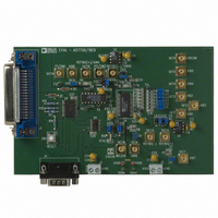
Manufacturer Part Number
EVAL-AD7708EBZ
Description
BOARD EVAL FOR AD7708
Manufacturer
Analog Devices Inc
Specifications of EVAL-AD7708EBZ
Number Of Adc's
1
Number Of Bits
16
Sampling Rate (per Second)
1.37k
Data Interface
Serial
Inputs Per Adc
8 Single or 4 Differential
Input Range
±2.5 V
Power (typ) @ Conditions
3.84mW @ 3 V
Voltage Supply Source
Analog and Digital
Operating Temperature
-40°C ~ 85°C
Utilized Ic / Part
AD7708
Lead Free Status / RoHS Status
Lead free / RoHS Compliant
Other names
EVAL-AD7708EB
EVAL-AD7708EB
EVAL-AD7708EB


AD0C2
AD0C1
AD0C0
Filter Register (A3, A2, A1, A0 = 0, 0, 1, 1; Power-On Reset = 45Hex)
The Filter Register is an 8-bit register from which data can be read or to which data can be written. This register determines the
amount of averaging performed by the sinc filter. Table XVII outlines the bit designations for the Filter Register. FR7 through FR0
indicate the bit location, FR denoting the bits are in the Filter Register. FR7 denotes the first bit of the data stream. The number in
brackets indicates the power-on/reset default status of that bit. The number in this register is used to set the decimation factor and
thus the output update rate for the ADCs. The filter register cannot be written to by the user the ADC is active. The update rate is
used for the ADCs is calculated as follows:
where
f
f
SF
The allowable range for SF is 13 decimal to 255 decimal with chop enabled, and the allowable SF range when chop is disabled is 03
decimal to 255 decimal. Examples of SF values and corresponding conversion rate (f
It should be noted that optimum performance is obtained when operating with chop enabled. When chopping is enabled (CHOP = 0),
the filter register is loaded with FF HEX during a calibration cycle. With chop disabled (CHOP =1), the value in the filter register is
used during calibration.
SF (Dec)
03
13
69
255
ADC
MOD
= ADC Output Update Rate,
= Modulator Clock Frequency = 32.768 kHz,
= Decimal Value Written to SF Register.
S
F
F
7
R
(
7
) 0
RN2
RN1
RN0
S
SF (Hex)
03
0D
45
FF
F
F
Table XVI. ADC Control Register (ADCCON) Bit Designations (continued)
6
R
6
(
) 1
ADC Range Bits
Written by the user to select the ADC input range as follows
RN2
0
0
0
0
1
1
1
1
S
F
F
f
f
ADC
ADC
5
R
Table XVII. Filter Register Bit Designations
(
5
) 0
=
=
Table XVIII. Update Rate vs. SF Word
1
3
8
RN1
0
0
1
1
0
0
1
1
f
N/A
105.3
19.79
5.35
ADC
×
×
1
SF
f
MOD
(Hz)
S
×
F
CHOP Enabled CHOP
F
4
f
R
MOD
CHOP Enabled
(
4
) 0
RN0
0
1
0
1
0
1
0
1
CHOP Disabled CHOP
S
F
F
3
Selected ADC Input Range (VREF = 2.5 V)
± 20 mV
± 40 mV
± 80 mV
± 160 mV
± 320 mV
± 640 mV
± 1.28 V
± 2.56 V
(
R
t
N/A
9.52
50.34
186.77
ADC
(
3
) 0
(ms)
(
=
0
ADC
S
)
F
F
) and time (t
2
=
R
(
1
2
) 1
)
f
1365.33
315
59.36
16.06
ADC
ADC
S
F
F
AD7708/AD7718
(Hz)
1
R
) are shown in Table XVIII.
(
1
) 0
CHOP Disabled
S
F
F
0
R
(
0
) 1
3.17
t
0.732
16.85
62.26
ADC
(ms)
Related parts for EVAL-AD7708EBZ
Image
Part Number
Description
Manufacturer
Datasheet
Request
R


Part Number:
Description:
BOARD EVAL FOR SI270X-A
Manufacturer:
Silicon Laboratories Inc
Datasheet:

Part Number:
Description:
BUCK CONV REF DESIGN KIT IP1201
Manufacturer:
International Rectifier
Datasheet:
Part Number:
Description:
BOARD DEMO SYNC DUAL BUCK CNVTER
Manufacturer:
International Rectifier
Datasheet:
Part Number:
Description:
BOARD DEMO SYNC BUCK CONVETER
Manufacturer:
International Rectifier
Datasheet:

Part Number:
Description:
EVALBOARD/EB Omnidirectional microphone - Analog
Manufacturer:
Analog Devices
Datasheet:
Part Number:
Description:
EVALBOARD/EB Omnidirectional microphone - Analog
Manufacturer:
Analog Devices
Datasheet:


Part Number:
Description:
BOARD EVAL LED DRIVER LT3756
Manufacturer:
Linear Technology
Datasheet:

Part Number:
Description:
BOARD EVAL FOR AD7741/7742
Manufacturer:
Analog Devices Inc
Datasheet:

Part Number:
Description:
±1.7g Dual-Axis IMEMS Accelerometer Evaluation Board
Manufacturer:
Analog Devices Inc
Datasheet:

Part Number:
Description:
IC MULTIPLIER ANALOG 8-SOIC T/R
Manufacturer:
Analog Devices Inc
Datasheet:

Part Number:
Description:
IC ANALOG MULTIPLIER 8-DIP
Manufacturer:
Analog Devices Inc
Datasheet:
Part Number:
Description:
IC ANALOG MULTIPLIER 8-SOIC
Manufacturer:
Analog Devices Inc
Datasheet:
Part Number:
Description:
IC ANALOG MULTIPLIER 8-DIP
Manufacturer:
Analog Devices Inc
Datasheet: