MCP3221DM-PCTL Microchip Technology, MCP3221DM-PCTL Datasheet - Page 19
MCP3221DM-PCTL
Manufacturer Part Number
MCP3221DM-PCTL
Description
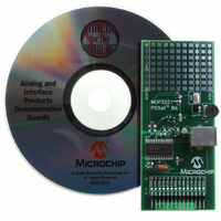
BOARD DEMO FOR PICTAIL MCP3221
Manufacturer
Microchip Technology
Series
PICtail™r
Type
A/Dr
Datasheets
1.MCP3221A5T-IOT.pdf
(28 pages)
2.MCP3221DM-PCTL.pdf
(20 pages)
3.MCP3221DM-PCTL.pdf
(20 pages)
Specifications of MCP3221DM-PCTL
Number Of Adc's
1
Number Of Bits
12
Sampling Rate (per Second)
22.3k
Data Interface
Serial
Inputs Per Adc
1 Single Ended
Voltage Supply Source
Single Supply
Operating Temperature
-40°C ~ 85°C
Utilized Ic / Part
MCP3221
Product
Data Conversion Development Tools
Resolution
12 bit
Interface Type
USB
Silicon Manufacturer
Microchip
Silicon Core Number
MCP3221
Kit Application Type
Data Converter
Application Sub Type
ADC
Silicon Family Name
PICtail
Kit Contents
Board Cables CD Docs
Rohs Compliant
Yes
For Use With/related Products
MCP3221
Lead Free Status / RoHS Status
Contains lead / RoHS non-compliant
Lead Free Status / RoHS Status
Lead free / RoHS Compliant, Contains lead / RoHS non-compliant
Available stocks
Company
Part Number
Manufacturer
Quantity
Price
Company:

Part Number:
MCP3221DM-PCTL
Manufacturer:
MICROCHIP
Quantity:
12 000


6.3
In some instances, it may be necessary to test for
MCP3221 presence on the I
a conversion. This operation is described in Figure 6-4.
Here we are setting the R/W bit in the address byte to
a zero. The MCP3221 will then acknowledge by pulling
SDA low during the ACK clock and then release the
bus back to the I
can then be issued from the master and I
communication can continue.
FIGURE 6-4:
6.4
6.4.1
V
erence voltage. A bypass capacitor value of 0.1 µF is
recommended. Adding a 10 µF capacitor in parallel is
recommended to attenuate higher frequency noise
present in some systems.
FIGURE 6-5:
6.4.2
When laying out a printed circuit board for use with
analog components, care should be taken to reduce
noise wherever possible. A bypass capacitor from
to ground should always be used with this device and
should be placed as close as possible to the device pin.
A bypass capacitor value of 0.1 µF is recommended.
© 2006 Microchip Technology Inc.
10 µF
DD
SDA
SCL
supplies the power to the device as well as the ref-
Start
Device Polling
Device Power and Layout
Considerations
Bit
A
0.1 µF
IN
POWERING THE
LAYOUT CONSIDERATIONS
Device bits
1 2 3 4 5 6 7 8 9
MCP3221
1 0 0
2
C master. A stop or repeated start bit
V
DD
Device Polling.
Powering the
V
Address Byte
DD
1
Address bits
A2 A1A0 0
SCL
SDA
2
C bus without performing
MCP3221
MCP3221 response
R
PU
R/W
V
MCP3221
DD
To
Microcontroller
R
PU
Start
Bit
.
V
2
DD
C
Digital and analog traces should be separated as much
as possible on the board, with no traces running
underneath the device or the bypass capacitor. Extra
precautions should be taken to keep traces with high-
frequency signals (such as clock lines) as far as
possible from analog traces.
Use of an analog ground plane is recommended in
order to keep the ground potential the same for all
devices on the board. Providing V
devices in a “star” configuration can also reduce noise
by eliminating current return paths and associated
errors (Figure 6-6). For more information on layout tips
when using the MCP3221 or other ADC devices, refer
to AN688, “Layout Tips for 12-Bit A/D Converter
Applications”.
FIGURE 6-6:
‘Star’ configuration in order to reduce errors
caused by current return paths.
6.4.3
The MCP3221 uses V
ence. In some applications, it may be necessary to use
a stable reference to achieve the required accuracy.
Figure 6-7 shows an example using the MCP1541 as a
4.096V, 2% reference.
FIGURE 6-7:
Reference Configuration.
Device 1
MCP1541
Reference
4.096V
USING A REFERENCE FOR
SUPPLY
V
DD
Device 2
C
Connection
L
1 µF
A
V
Stable Power and
DD
IN
DD
V
as both power and a refer-
MCP3221
DD
traces arranged in a
MCP3221
SDA
SCL
V
Device 3
DD
DD
DS21732C-page 19
connections to
Device 4
R
PU
V
DD
Related parts for MCP3221DM-PCTL
Image
Part Number
Description
Manufacturer
Datasheet
Request
R

Part Number:
Description:
Manufacturer:
Microchip Technology Inc.
Datasheet:
Part Number:
Description:
Manufacturer:
Microchip Technology Inc.
Datasheet:
Part Number:
Description:
Manufacturer:
Microchip Technology Inc.
Datasheet:
Part Number:
Description:
Manufacturer:
Microchip Technology Inc.
Datasheet:
Part Number:
Description:
Manufacturer:
Microchip Technology Inc.
Datasheet:
Part Number:
Description:
Manufacturer:
Microchip Technology Inc.
Datasheet:
Part Number:
Description:
Manufacturer:
Microchip Technology Inc.
Datasheet:
Part Number:
Description:
Manufacturer:
Microchip Technology Inc.
Datasheet: