MCP3221DM-PCTL Microchip Technology, MCP3221DM-PCTL Datasheet - Page 12
MCP3221DM-PCTL
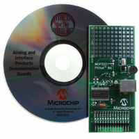
Manufacturer Part Number
MCP3221DM-PCTL
Description
BOARD DEMO FOR PICTAIL MCP3221
Manufacturer
Microchip Technology
Series
PICtail™r
Type
A/Dr
Datasheets
1.MCP3221A5T-IOT.pdf
(28 pages)
2.MCP3221DM-PCTL.pdf
(20 pages)
3.MCP3221DM-PCTL.pdf
(20 pages)
Specifications of MCP3221DM-PCTL
Number Of Adc's
1
Number Of Bits
12
Sampling Rate (per Second)
22.3k
Data Interface
Serial
Inputs Per Adc
1 Single Ended
Voltage Supply Source
Single Supply
Operating Temperature
-40°C ~ 85°C
Utilized Ic / Part
MCP3221
Product
Data Conversion Development Tools
Resolution
12 bit
Interface Type
USB
Silicon Manufacturer
Microchip
Silicon Core Number
MCP3221
Kit Application Type
Data Converter
Application Sub Type
ADC
Silicon Family Name
PICtail
Kit Contents
Board Cables CD Docs
Rohs Compliant
Yes
For Use With/related Products
MCP3221
Lead Free Status / RoHS Status
Contains lead / RoHS non-compliant
Lead Free Status / RoHS Status
Lead free / RoHS Compliant, Contains lead / RoHS non-compliant
Available stocks
Company
Part Number
Manufacturer
Quantity
Price
Company:

Part Number:
MCP3221DM-PCTL
Manufacturer:
MICROCHIP
Quantity:
12 000


MCP3221
3.0
TABLE 3-1:
3.1
The V
device as well as a voltage reference for the conversion
process. Refer to Section 6.4 “Device Power and
Layout Considerations”, “Device Power and Layout
Considerations”, for tips on power and grounding.
3.2
AIN is the input pin to the sample-and-hold circuitry of
the Successive Approximation Register (SAR) con-
verter. Care should be taken in driving this pin. Refer to
Section 6.1 “Driving the Analog Input”, “Driving the
Analog Input”. For proper conversions, the voltage on
this pin can vary from V
DS21732C-page 12
DD
Name
SDA
SCL
V
V
A
DD
SS
PIN FUNCTIONS
IN
V
pin, with respect to V
Analog Input (A
DD
and V
PIN FUNCTION TABLE
+2.7V to 5.5V Power Supply
Ground
Analog Input
Serial Data In/Out
Serial Clock In
SS
SS
to V
SS
IN
DD
Function
)
, provides power to the
.
3.3
SDA is a bidirectional pin used to transfer addresses
and data into and out of the device. Since it is an open-
drain terminal, the SDA bus requires a pull-up resistor
to V
400 kHz SCL clock speeds). Refer to Section 6.2
“Connecting to the I
Bus”, for more information.
For normal data transfer, SDA is allowed to change only
during SCL low. Changes during SCL high are reserved
for indicating the START and STOP conditions. Refer to
Section 5.1 “I
Characteristics”.
3.4
SCL is an input pin used to synchronize the data trans-
fer to and from the device on the SDA pin and is an
open-drain terminal. Therefore, the SCL bus requires a
pull-up resistor to V
2 kΩ for 400 kHz SCL clock speeds. Refer to
Section 6.2 “Connecting to the I
ing to the I
For normal data transfer, SDA is allowed to change
only during SCL low. Changes during SCL high are
reserved for indicating the START and STOP
conditions. Refer to Section 6.1 “Driving the Analog
Input”, “Driving the Analog Input”.
DD
(typically 10 kΩ for 100 kHz and 2 kΩ for
Serial Data (SDA)
Serial Clock (SCL)
2
C Bus”).
2
C Bus Characteristics”, “I
DD
2
(typically 10 kΩ for 100 kHz and
C Bus”, “Connecting to the I
© 2006 Microchip Technology Inc.
2
C Bus”, “Connect-
2
C Bus
2
C
Related parts for MCP3221DM-PCTL
Image
Part Number
Description
Manufacturer
Datasheet
Request
R

Part Number:
Description:
Manufacturer:
Microchip Technology Inc.
Datasheet:
Part Number:
Description:
Manufacturer:
Microchip Technology Inc.
Datasheet:
Part Number:
Description:
Manufacturer:
Microchip Technology Inc.
Datasheet:
Part Number:
Description:
Manufacturer:
Microchip Technology Inc.
Datasheet:
Part Number:
Description:
Manufacturer:
Microchip Technology Inc.
Datasheet:
Part Number:
Description:
Manufacturer:
Microchip Technology Inc.
Datasheet:
Part Number:
Description:
Manufacturer:
Microchip Technology Inc.
Datasheet:
Part Number:
Description:
Manufacturer:
Microchip Technology Inc.
Datasheet: