CDB5376 Cirrus Logic Inc, CDB5376 Datasheet - Page 16
CDB5376
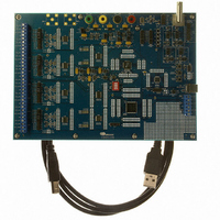
Manufacturer Part Number
CDB5376
Description
EVALUATION BOARD FOR CS5376
Manufacturer
Cirrus Logic Inc
Datasheets
1.CS5371A-ISZR.pdf
(32 pages)
2.CS4373A-ISZ.pdf
(34 pages)
3.CS5376A-IQZR.pdf
(106 pages)
4.CDB5378.pdf
(16 pages)
5.CDB5376.pdf
(80 pages)
6.CDB5376.pdf
(16 pages)
Specifications of CDB5376
Main Purpose
Seismic Evaluation System
Embedded
Yes, MCU, 8-Bit
Utilized Ic / Part
CS3301A, CS3302A, CS4373A, CS5372A, CS5376A
Primary Attributes
Quad Digital Filter
Secondary Attributes
Graphical User Interface, SPI™ & USB Interfaces
Processor To Be Evaluated
CS330x, CS4373A, CS537x
Interface Type
USB
Lead Free Status / RoHS Status
Contains lead / RoHS non-compliant
Lead Free Status / RoHS Status
Lead free / RoHS Compliant, Contains lead / RoHS non-compliant
Other names
598-1778


4. ANALOG SIGNALS
The CS5371A and CS5372A modulators have
differential analog inputs which are separated
into rough and fine charge differential pairs
(INR±, INF±) to maximize sampling accuracy.
Both sets of modulator inputs require a simple
differential anti-alias RC filter to ensure high-
frequency signals do not alias into the mea-
surement bandwidth.
4.1 INR±, INF± Modulator Inputs
The modulator analog inputs are separated
into differential rough and fine signals (INR±,
INF±). The positive half of the differential input
signal is connected to INR+ and INF+, while
the negative half is attached to INF- and INR-.
The INR± pins are switched-capacitor ‘rough
charge’ inputs that pre-charge the internal an-
alog sampling capacitor before it is connected
to the INF± fine input pins.
16
VA+
VA+
VA-
VA-
VA+
VA+
VA-
VA-
AMPLIFIER
AMPLIFIER
CS3301A
CS3302A
CS3301A
CS3302A
VA+
VA-
OUTR+
OUTF+
OUTF-
OUTR-
OUTR+
OUTF+
OUTF-
OUTR-
VREF
2.5 V
680
680
680
680
680
680
680
680
10 Ω
100μF
20nF
20nF
C0G
C0G
Figure 11. Analog Signals
VA+
VA-
0.01μF
20nF
C0G
20nF
C0G
INR+
INF+
INF-
INR-
VREF+
VREF-
INR-
INF-
INF+
INR+
0.1μF
0.1μF
4.2 Input Impedance
The modulator inputs have a dynamic
switched-capacitor architecture and so have a
rough charge input impedance that is inversely
proportional to the input master clock frequen-
cy and the input capacitor size, [1 / (f x C)].
Internal to the modulator, the rough inputs
(INR±) pre-charge the sampling capacitor
used by the fine inputs (INF±), therefore the in-
put current to the fine inputs is typically very
low and the effective input impedance is or-
ders of magnitude above the impedance of the
rough inputs.
VA+
ΔΣ Modulator
VA-
•
•
•
CS5372A
MCLK = 2.048 MHz
INR± Internal Input Capacitor = 20 pF
Impedance = [1 / (2.048 MHz * 20 pF)] = 24 kΩ.
GND
VD
MDATA2
MFLAG2
MDATA1
MFLAG1
MSYNC
PWDN2
PWDN1
0.01μF
MCLK
OFST
VD
CS5371A CS5372A
MDATA1
MFLAG1
GPIO
MCLK
MSYNC
GPIO
MDATA2
MFLAG2
GPIO
Digital Filter
CS5376A
VDD2
GND
VD
DS748F3
Related parts for CDB5376
Image
Part Number
Description
Manufacturer
Datasheet
Request
R

Part Number:
Description:
Development Kit
Manufacturer:
Cirrus Logic Inc
Datasheet:
Part Number:
Description:
Development Kit
Manufacturer:
Cirrus Logic Inc
Datasheet:


Part Number:
Description:
High-efficiency PFC + Fluorescent Lamp Driver Reference Design
Manufacturer:
Cirrus Logic Inc
Datasheet:
Part Number:
Description:
Development Kit
Manufacturer:
Cirrus Logic Inc
Datasheet:
Part Number:
Description:
Development Kit
Manufacturer:
Cirrus Logic Inc
Datasheet:

Part Number:
Description:
Development Kit
Manufacturer:
Cirrus Logic Inc
Datasheet:
Part Number:
Description:
Development Kit
Manufacturer:
Cirrus Logic Inc
Datasheet:
Part Number:
Description:
Development Kit
Manufacturer:
Cirrus Logic Inc
Datasheet:
Part Number:
Description:
Development Kit
Manufacturer:
Cirrus Logic Inc
Datasheet:

Part Number:
Description:
EVALUATION BOARD FOR CS8427
Manufacturer:
Cirrus Logic Inc
Datasheet:

Part Number:
Description:
BOARD EVAL FOR CS8416 RCVR
Manufacturer:
Cirrus Logic Inc
Datasheet:

Part Number:
Description:
EVALUATION BOARD FOR CS8420
Manufacturer:
Cirrus Logic Inc
Datasheet:

Part Number:
Description:
KIT DEVELOPMENT EP9315 ARM9
Manufacturer:
Cirrus Logic Inc
Datasheet:

Part Number:
Description:
KIT DEVELOPMENT EP9302 ARM9
Manufacturer:
Cirrus Logic Inc
Datasheet: