CDB42L51 Cirrus Logic Inc, CDB42L51 Datasheet - Page 5
CDB42L51
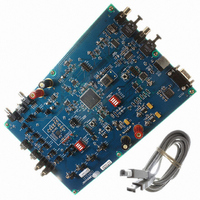
Manufacturer Part Number
CDB42L51
Description
BOARD EVAL FOR CS42L51 CODEC
Manufacturer
Cirrus Logic Inc
Specifications of CDB42L51
Main Purpose
Audio, CODEC
Embedded
Yes, Other
Utilized Ic / Part
CS42L51, CS8406, CS8415
Primary Attributes
Stereo, Digital Audio Transmitter and Receiver
Secondary Attributes
Graphic User Interface, S/PDIF Interface
Description/function
Audio CODECs
Operating Supply Voltage
5 V
Product
Audio Modules
For Use With/related Products
CS42L51
Lead Free Status / RoHS Status
Contains lead / RoHS non-compliant
Lead Free Status / RoHS Status
Lead free / RoHS Compliant, Contains lead / RoHS non-compliant
Other names
598-1005


CS42L51
11. PARAMETER DEFINITIONS .............................................................................................................. 83
12. PACKAGE DIMENSIONS ................................................................................................................. 84
THERMAL CHARACTERISTICS ........................................................................................................ 84
13. ORDERING INFORMATION ............................................................................................................. 85
14. REFERENCES .................................................................................................................................... 85
15. REVISION HISTORY ......................................................................................................................... 86
LIST OF FIGURES
Figure 1.Typical Connection Diagram (Software Mode) ........................................................................... 10
Figure 2.Typical Connection Diagram (Hardware Mode) .......................................................................... 11
Figure 3.Headphone Output Test Load ..................................................................................................... 19
Figure 4.Serial Audio Interface Slave Mode Timing .................................................................................. 21
Figure 5.Serial Audio Interface Master Mode Timing ................................................................................ 21
Figure 6.Control Port Timing - I²C ............................................................................................................. 22
Figure 7.Control Port Timing - SPI Format ................................................................................................ 23
Figure 8.Analog Input Architecture ............................................................................................................ 28
Figure 9.MIC Input Mix w/Common Mode Rejection ................................................................................. 30
Figure 10.Differential Input ........................................................................................................................ 30
Figure 11.ALC ........................................................................................................................................... 32
Figure 12.Noise Gate Attenuation ............................................................................................................. 33
Figure 13.Output Architecture ................................................................................................................... 34
Figure 14.De-Emphasis Curve .................................................................................................................. 35
Figure 15.Beep Configuration Options ...................................................................................................... 36
Figure 16.Peak Detect & Limiter ............................................................................................................... 37
Figure 17.Master Mode Timing ................................................................................................................. 39
Figure 18.Tri-State Serial Port .................................................................................................................. 40
Figure 19.I²S Format ................................................................................................................................. 40
Figure 20.Left-Justified Format ................................................................................................................. 41
Figure 21.Right-Justified Format (DAC only) ............................................................................................ 41
Figure 22.Initialization Flowchart ............................................................................................................... 42
Figure 23.Control Port Timing in SPI Mode .............................................................................................. 43
Figure 24.Control Port Timing, I²C Write ................................................................................................... 44
Figure 25.Control Port Timing, I²C Read ................................................................................................... 44
Figure 26.AIN & PGA Selection ................................................................................................................ 56
Figure 27.THD+N vs. Output Power per Channel at 1.8 V (16 Ω load) .................................................... 75
Figure 28.THD+N vs. Output Power per Channel at 2.5 V (16 Ω load) .................................................... 75
Figure 29.THD+N vs. Output Power per Channel at 1.8 V (32 Ω load) .................................................... 76
Figure 30.THD+N vs. Output Power per Channel at 2.5 V (32 Ω load) .................................................... 76
Figure 31.Power Dissipation vs. Output Power into Stereo 16 Ω ......................................................................77
Figure 32.Power Dissipation vs. Output Power into Stereo 16 Ω (Log Detail) .......................................... 77
Figure 33.ADC THD+N vs. Frequency w/Capacitor Effects ...................................................................... 78
Figure 34.ADC Passband Ripple .............................................................................................................. 82
Figure 35.ADC Stopband Rejection .......................................................................................................... 82
Figure 36.ADC Transition Band ................................................................................................................ 82
Figure 37.ADC Transition Band Detail ...................................................................................................... 82
Figure 38.DAC Passband Ripple .............................................................................................................. 82
Figure 39.DAC Stopband .......................................................................................................................... 82
Figure 40.DAC Transition Band ................................................................................................................ 82
Figure 41.DAC Transition Band (Detail) .................................................................................................... 82
DS679F1
5
Related parts for CDB42L51
Image
Part Number
Description
Manufacturer
Datasheet
Request
R

Part Number:
Description:
Development Kit
Manufacturer:
Cirrus Logic Inc
Datasheet:
Part Number:
Description:
Development Kit
Manufacturer:
Cirrus Logic Inc
Datasheet:


Part Number:
Description:
High-efficiency PFC + Fluorescent Lamp Driver Reference Design
Manufacturer:
Cirrus Logic Inc
Datasheet:
Part Number:
Description:
Development Kit
Manufacturer:
Cirrus Logic Inc
Datasheet:
Part Number:
Description:
Development Kit
Manufacturer:
Cirrus Logic Inc
Datasheet:

Part Number:
Description:
Development Kit
Manufacturer:
Cirrus Logic Inc
Datasheet:
Part Number:
Description:
Development Kit
Manufacturer:
Cirrus Logic Inc
Datasheet:
Part Number:
Description:
Development Kit
Manufacturer:
Cirrus Logic Inc
Datasheet:
Part Number:
Description:
Development Kit
Manufacturer:
Cirrus Logic Inc
Datasheet:

Part Number:
Description:
EVALUATION BOARD FOR CS8427
Manufacturer:
Cirrus Logic Inc
Datasheet:

Part Number:
Description:
BOARD EVAL FOR CS8416 RCVR
Manufacturer:
Cirrus Logic Inc
Datasheet:

Part Number:
Description:
EVALUATION BOARD FOR CS8420
Manufacturer:
Cirrus Logic Inc
Datasheet:

Part Number:
Description:
KIT DEVELOPMENT EP9315 ARM9
Manufacturer:
Cirrus Logic Inc
Datasheet:

Part Number:
Description:
KIT DEVELOPMENT EP9302 ARM9
Manufacturer:
Cirrus Logic Inc
Datasheet: