CDB42L51 Cirrus Logic Inc, CDB42L51 Datasheet - Page 41
CDB42L51
Manufacturer Part Number
CDB42L51
Description
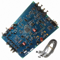
BOARD EVAL FOR CS42L51 CODEC
Manufacturer
Cirrus Logic Inc
Specifications of CDB42L51
Main Purpose
Audio, CODEC
Embedded
Yes, Other
Utilized Ic / Part
CS42L51, CS8406, CS8415
Primary Attributes
Stereo, Digital Audio Transmitter and Receiver
Secondary Attributes
Graphic User Interface, S/PDIF Interface
Description/function
Audio CODECs
Operating Supply Voltage
5 V
Product
Audio Modules
For Use With/related Products
CS42L51
Lead Free Status / RoHS Status
Contains lead / RoHS non-compliant
Lead Free Status / RoHS Status
Lead free / RoHS Compliant, Contains lead / RoHS non-compliant
Other names
598-1005


DS679F1
4.7
4.8
LRCK
SCLK
LRCK
SCLK
SDIN
SDIN
Initialization
The initialization and Power-Down sequence flowchart is shown in
ters a Power-Down state upon initial power-up. The interpolation and decimation filters, delta-sigma modu-
lators and control port registers are reset. The internal voltage reference, multi-bit DAC and ADC and
switched-capacitor low-pass filters are powered down.
The device will remain in the Power-Down state until the RESET pin is brought high. The control port is ac-
cessible once RESET is high and the desired register settings can be loaded per the interface descriptions
in
10 ms, the CODEC will enter Hardware Mode.
Once MCLK is valid, the quiescent voltage, VQ, and the internal voltage references, DAC_FILT+ and
ADC_FILT+ will begin powering up to normal operation. The charge pump slowly powers up and charges
the capacitors. Power is then applied to the headphone amplifiers and switched-capacitor filters, and the an-
alog/digital outputs enter a muted state. Once LRCK is valid, MCLK occurrences are counted over one LRCK
period to determine the MCLK/LRCK frequency ratio and normal operation begins.
Recommended Power-Up Sequence
1. Hold RESET low until the power supplies are stable.
2. Bring RESET high. After approximately 10 ms, the device will enter Hardware Mode.
3. For Software Mode operation, set the PDN bit to ‘1’b in under 10 ms. This will place the device in “stand-
4. Load the desired register settings while keeping the PDN bit set to ‘1’b.
5. Start MCLK to the appropriate frequency, as discussed in
6. Set the PDN bit to ‘0’b.
7. Apply LRCK,SCLK and SDIN for normal operation to begin.
8. Bring RESET low if the analog or digital supplies drop below the recommended operating condition to
M S B
“Software Mode” on page
by”.
prevent power glitch related issues.
AOUTA / AINxA
L eft C h a n n e l
AOUTA
L eft C h a n n el
M S B
Figure 21. Right-Justified Format (DAC only)
43. If a valid write sequence to the control port is not made within approximately
Figure 20. Left-Justified Format
L S B
L S B
M S B
Section
AOUTB / AINxB
R ig ht C h a n n e l
Figure 22 on page
4.5.
R ig ht C h a n n el
AOUTB
M S B
42. The CODEC en-
L S B
CS42L51
MSB
L S B
41
Related parts for CDB42L51
Image
Part Number
Description
Manufacturer
Datasheet
Request
R

Part Number:
Description:
Development Kit
Manufacturer:
Cirrus Logic Inc
Datasheet:
Part Number:
Description:
Development Kit
Manufacturer:
Cirrus Logic Inc
Datasheet:


Part Number:
Description:
High-efficiency PFC + Fluorescent Lamp Driver Reference Design
Manufacturer:
Cirrus Logic Inc
Datasheet:
Part Number:
Description:
Development Kit
Manufacturer:
Cirrus Logic Inc
Datasheet:
Part Number:
Description:
Development Kit
Manufacturer:
Cirrus Logic Inc
Datasheet:

Part Number:
Description:
Development Kit
Manufacturer:
Cirrus Logic Inc
Datasheet:
Part Number:
Description:
Development Kit
Manufacturer:
Cirrus Logic Inc
Datasheet:
Part Number:
Description:
Development Kit
Manufacturer:
Cirrus Logic Inc
Datasheet:
Part Number:
Description:
Development Kit
Manufacturer:
Cirrus Logic Inc
Datasheet:

Part Number:
Description:
EVALUATION BOARD FOR CS8427
Manufacturer:
Cirrus Logic Inc
Datasheet:

Part Number:
Description:
BOARD EVAL FOR CS8416 RCVR
Manufacturer:
Cirrus Logic Inc
Datasheet:

Part Number:
Description:
EVALUATION BOARD FOR CS8420
Manufacturer:
Cirrus Logic Inc
Datasheet:

Part Number:
Description:
KIT DEVELOPMENT EP9315 ARM9
Manufacturer:
Cirrus Logic Inc
Datasheet:

Part Number:
Description:
KIT DEVELOPMENT EP9302 ARM9
Manufacturer:
Cirrus Logic Inc
Datasheet: