CDB42L51 Cirrus Logic Inc, CDB42L51 Datasheet
CDB42L51
Specifications of CDB42L51


Related parts for CDB42L51


CDB42L51 Summary of contents
Page 1
Low Power, Stereo CODEC with Headphone Amp DIGITAL to ANALOG FEATURES 98 dB Dynamic Range (A-wtd) -86 dB THD+N Headphone Amplifier - GND Centered – On-Chip Charge Pump Provides -VA_HP – No DC-Blocking Capacitor Required 46 mW Power Into Stereo ...
Page 2
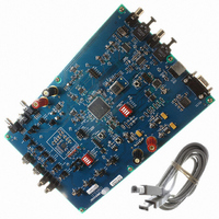
... The CS42L51 is available in a 32-pin QFN package in both Commercial (-10 to +70° C) and Automotive grades (-40 to +85° C). The CDB42L51 Customer Dem- onstration board is also available for device evaluation and implementation suggestions. Please see Information” on page 85 CS42L51 “ ...
Page 3
TABLE OF CONTENTS 1. PIN DESCRIPTIONS - SOFTWARE (HARDWARE) MODE .................................................................. 7 1.1 Digital I/O Pin Characteristics ........................................................................................................... 9 2. TYPICAL CONNECTION DIAGRAMS ................................................................................................. 10 3. CHARACTERISTIC AND SPECIFICATION TABLES ......................................................................... 12 SPECIFIED OPERATING CONDITIONS ............................................................................................. 12 ABSOLUTE MAXIMUM RATINGS ...
Page 4
High-Impedance Digital Output ............................................................................................. 40 4.5.4 Quarter- and Half-Speed Mode ............................................................................................. 40 4.6 Digital Interface Formats ................................................................................................................ 40 4.7 Initialization ..................................................................................................................................... 41 4.8 Recommended Power-Up Sequence ............................................................................................. 41 4.9 Recommended Power-Down Sequence ........................................................................................ 42 4.10 Software Mode ............................................................................................................................. 43 ...
Page 5
PARAMETER DEFINITIONS .............................................................................................................. 83 12. PACKAGE DIMENSIONS ................................................................................................................. 84 THERMAL CHARACTERISTICS ........................................................................................................ 84 13. ORDERING INFORMATION ............................................................................................................. 85 14. REFERENCES .................................................................................................................................... 85 15. REVISION HISTORY ......................................................................................................................... 86 LIST OF FIGURES Figure 1.Typical Connection Diagram (Software Mode) ........................................................................... 10 Figure ...
Page 6
LIST OF TABLES Table 1. I/O Power Rails ............................................................................................................................. 9 Table 2. Hardware Mode Feature Summary ............................................................................................. 27 Table 3. MCLK/LRCK Ratios .................................................................................................................... 39 6 CS42L51 DS679F1 ...
Page 7
PIN DESCRIPTIONS - SOFTWARE (HARDWARE) MODE LRCK SDA/CDIN (MCLKDIV2) SCL/CCLK (I²S/LJ) ADO/CS (DEM) VA_HP FLYP GND_HP FLYN Pin Name # Left Right Clock (Input/Output) - Determines which channel, Left or Right, is currently active on the 1 LRCK serial ...
Page 8
AOUTB Analog Audio Output (Output) - The full-scale output level is specified in the DAC Analog Characteris- 11 AOUTA tics specification table 12 VA Analog Power (Input) - Positive power for the internal analog section. 13 AGND Analog Ground ...
Page 9
Digital I/O Pin Characteristics The logic level for each input should not exceed the maximum ratings for the VL power supply. Pin Name I/O SW/(HW) RESET Input SCL/CCLK Input (I²S/LJ) SDA/CDIN Input/Output (MCLKDIV2) AD0/CS Input (DEM) MCLK Input LRCK ...
Page 10
TYPICAL CONNECTION DIAGRAMS +1 +2 µF 0.1 µ 1.5 µF 1 µF See Note 1.5 µF 1 µF * *Use low ESR ceramic capacitors. Note 2 : For best response ...
Page 11
FLYP ** 1 µF FLYN VSS_HP ** 1 µF GND_HP * *Use low ESR ceramic capacitors. MCLK SCLK LRCK SDIN VL or DGND (1) SDOUT/ Digital Audio M/S Processor RESET I²S/LJ MCLKDIV2 DEM ...
Page 12
CHARACTERISTIC AND SPECIFICATION TABLES (All Min/Max characteristics and specifications are guaranteed over the Specified Operating Conditions. Typical per- formance characteristics and specifications are derived from measurements taken at nominal supply voltages and T = 25° C.) A SPECIFIED OPERATING ...
Page 13
ANALOG INPUT CHARACTERISTICS (COMMERCIAL - CNZ) (Test Conditions (unless otherwise specified): Input sine wave (relative to digital full scale): 1 kHz through passive input filter; Measurement Bandwidth kHz unless otherwise specified. Sample Frequency = 48 ...
Page 14
ANALOG INPUT CHARACTERISTICS (AUTOMOTIVE - DNZ) (Test Conditions (unless otherwise specified): Input sine wave (relative to full scale): 1 kHz through passive input filter; Measurement Bandwidth kHz unless otherwise specified. Sample Frequency = 48 kHz) ...
Page 15
Referred to the typical full-scale voltage. Applies to all THD+N and Dynamic Range values in the table. 6. Measured between AINxx and AGND. ADC DIGITAL FILTER CHARACTERISTICS Parameter Passband (Frequency Response) Passband Ripple Stopband Stopband Attenuation Total Group Delay ...
Page 16
ANALOG OUTPUT CHARACTERISTICS (COMMERCIAL - CNZ) (Test conditions (unless otherwise specified): Input test signal is a full-scale 997 Hz sine wave; measurement bandwidth kHz; Sample Frequency = 48 kHz; test load Ω, ...
Page 17
ANALOG OUTPUT CHARACTERISTICS (AUTOMOTIVE - DNZ) (Test conditions (unless otherwise specified): Input test signal is a full-scale 997 Hz sine wave; measurement bandwidth kHz; Sample Frequency = 48 kHz and 96 kHz; test load R ...
Page 18
LINE OUTPUT VOLTAGE CHARACTERISTICS Test conditions (unless otherwise specified): Input test signal is a full-scale 997 Hz sine wave; measurement band- width kHz; Sample Frequency = 48 kHz; test load R Parameter Ω AOUTx Voltage ...
Page 19
HEADPHONE OUTPUT POWER CHARACTERISTICS Test conditions (unless otherwise specified): Input test signal is a full-scale 997 Hz sine wave; measurement band- width kHz; Sample Frequency = 48 kHz; test load R Parameter Ω AOUTx Power ...
Page 20
COMBINED DAC INTERPOLATION & ON-CHIP ANALOG FILTER RESPONSE Parameter Frequency Response kHz Passband StopBand StopBand Attenuation (Note 13) Group Delay De-emphasis Error Notes: 12. Response is clock dependent and will scale with Fs. Note that the ...
Page 21
Parameters Master Mode (Note 17) Output Sample Rate (LRCK) LRCK Duty Cycle SCLK Frequency SCLK Duty Cycle LRCK Edge to SDOUT MSB Output Delay SDOUT Setup Time Before SCLK Rising Edge SDOUT Hold Time After SCLK Rising Edge SDIN Setup ...
Page 22
SWITCHING SPECIFICATIONS - I²C (Inputs: Logic 0 = DGND, Logic 1 = VL, SDA C Parameter SCL Clock Frequency RESET Rising Edge to Start Bus Free Time Between Transmissions Start Condition Hold Time (prior to first clock pulse) Clock Low ...
Page 23
SWITCHING CHARACTERISTICS - SPI (Inputs: Logic 0 = DGND, Logic 1 = VL) Parameter CCLK Clock Frequency RESET Rising Edge to CS Falling CS Falling to CCLK Edge CS High Time Between Transmissions CCLK Low Time CCLK High Time CDIN ...
Page 24
DC ELECTRICAL CHARACTERISTICS (AGND = 0 V; all voltages with respect to ground.) Parameters VQ Characteristics Nominal Voltage Output Impedance DC Current Source/Sink (Note 22) DAC_FILT+ Nominal Voltage ADC_FILT+ Nominal Voltage VSS_HP Characteristics Nominal Voltage DC Current Source MIC BIAS ...
Page 25
POWER CONSUMPTION See (Note 25) Operation 1 Off (Note 26) 2 Standby (Note 27) ADC 1.8 3 Mono Record PGA to ADC ...
Page 26
APPLICATIONS 4.1 Overview 4.1.1 Architecture The is a highly integrated, low power, 24-bit audio CODEC comprised of stereo analog-to-digital CS42L51 converters (ADC), and stereo digital-to-analog converters (DAC) designed using multi-bit delta-sigma techniques. The DAC operates at an oversampling ratio ...
Page 27
Hardware Mode A limited feature-set is available when the CODEC powers up in Hardware Mode (see er-Up Sequence” on page functions/features, the default configuration and the associated stand-alone control available. Hardware Mode Feature/Function Summary Feature/Function Power Control MICx Pre-amplifier ...
Page 28
Analog Inputs AINxA and AINxB are the analog inputs, internally biased to VQ, that accepts line-level and MIC-level sig- nals, allowing various gain and signal adjustments for each channel. MUX MUX ADCA_HPF FREEZE ADCA_HPF ENABLE ALC_ARATE[5:0] ALC_RRATE[5:0] Σ MICMIX ...
Page 29
High-Pass Filter and DC Offset Calibration The high-pass filter continuously subtracts a measure of the DC offset from the output of the decimation filter. If the high-pass filter is “frozen” during normal operation, the current value of the DC ...
Page 30
The MICBIAS series resistor must be selected based on the requirements of the particular microphone used. The MICBIAS output pin is selected using the MICBIAS_SEL bit. Software “Interface Control (Address 04h)” on page Controls Figure 9. MIC Input ...
Page 31
Analog Input Multiplexer A stereo 4-to-1 analog input multiplexer selects between a line-level input source mic-level input source, depending on the PDN_PGAx and AINx_MUX[1:0] bit settings. Signals may be routed to or by- passed around the PGA. ...
Page 32
Automatic Level Control (ALC) When enabled, the ALC monitors the analog input signal after the digital attenuator, detects when peak levels exceed the maximum threshold settings and lowers, first, the PGA gain settings and then increases the digital attenuation ...
Page 33
Noise Gate The noise gate may be used to mute signal levels that fall below a programmable threshold. This prevents the ALC from applying gain to noise. A programmable delay may be used to set the minimum time before ...
Page 34
Analog Outputs AOUTA and AOUTB are the ground-centered line or headphone outputs. Various signal processing options are available, including digital mixes with the ADC signal and an internal Beep Generator. The desired path to the DAC must be selected ...
Page 35
Gain -10dB 4.4.2 Volume Controls Three digital volume control functions are implemented, offering independent control over the ADC and PCM signal paths into the mixer as well as a combined control over the mixed signals. All volume controls are programmable ...
Page 36
CONTINUOUS BEEP: Beep turns configurable frequency (FREQ) and volume (BPVOL) and remains REPEAT = '1' on until REPEAT is cleared. BEEP = '1' MULTI-BEEP: Beep turns configurable frequency (FREQ) REPEAT = '1' and volume ...
Page 37
Input MAX[2:0] Limiter Volume Output (after Limiter) MAX[2:0] 4.4.7 Line-Level Outputs and Filtering The CODEC contains on-chip buffer amplifiers capable of producing line level single-ended outputs on AOUTA and AOUTB. These amplifiers are ground centered and do not have any ...
Page 38
On-Chip Charge Pump An on-chip charge pump derives a negative supply voltage from the VA_HP supply. This provides dual rail supplies allowing a full-scale output swing centered around ground and eliminates the need for large, DC-blocking capacitors. Added benefits ...
Page 39
Slave LRCK and SCLK are inputs in Slave Mode. The speed of the CODEC is automatically determined based on the input MCLK/LRCK ratio when the Auto-Detect function is enabled. Certain input clock ratios will then require an internal divide-by-two ...
Page 40
High-Impedance Digital Output The serial port may be placed on a clock/data bus that allows multiple masters for the serial port I/O with- out the need for external buffers. The 3ST_SP bit places the internal buffers for these I/O ...
Page 41
LRCK L eft SCLK SDIN AOUTA / AINxA LRCK L eft SCLK SDIN AOUTA 4.7 Initialization The initialization and Power-Down sequence ...
Page 42
Recommended Power-Down Sequence To minimize audible pops when turning off or placing the CODEC in standby, 1. Mute the DAC’s and ADC’s. 2. Set the PDN bit in the power control register to ‘1’b. The CODEC will not power ...
Page 43
Software Mode The control port is used to access the registers allowing the CODEC to be configured for the desired oper- ational modes and formats. The operation of the control port may be completely asynchronous with respect to the ...
Page 44
MAP will be output. Setting the auto-increment bit in MAP allows successive reads or writes of consecutive registers. Each byte is separated by an acknowledge bit. The ACK bit is output ...
Page 45
Memory Address Pointer (MAP) The MAP byte comes after the address byte and selects the register to be read or written. Refer to the pseudo code above for implementation details. 4.10.3.1 Map Increment (INCR) The device has MAP auto-increment ...
Page 46
REGISTER QUICK REFERENCE Software mode register defaults are as shown. “Reserved” registers must maintain their default state. Addr Function 7 01h ID Chip_ID4 Chip_ID3 default 02h Power Ctl. 1 Reserved PDN_DACB PDN_DACA dPDN_PGAB PDN_PGAA 0 p ...
Page 47
Addr Function default 0Eh Vol. Control MUTE_ADC ADCMIXA ADCMIXA MIXA default 0Fh Vol. Control MUTE_ADC ADCMIXB ADCMIXB MIXB default 10h Vol. Control MUTE_PCM PCMMIXA PCMMIXA MIXA default ...
Page 48
Addr Function 7 1Ah Limiter Con- LIMIT_EN LIMIT_ALL fig & Release Rate default 1Bh Limiter Attack Reserved Reserved Rate default 1Ch ALC Enable ALC_ENB ALC_ENA & Attack Rate default 1Dh ALC ...
Page 49
REGISTER DESCRIPTION All registers are read/write except for the chip I.D. and Revision Register and Interrupt Status Register which are read only. See the following bit definition tables for bit assignment information. The default state of each bit after ...
Page 50
Power Down PGA X (PDN_PGAX) Default Disable 1 - Enable Function: PGA channel x will either enter a power-down or muted state when this bit is enabled. See 1 (Address 02h) on page 49 This bit is ...
Page 51
Speed Mode (SPEED[1:0]) Default Quarter-Speed Mode (QSM 12.5 kHz sample rates 10 - Half-Speed Mode (HSM kHz sample rates 01 - Single-Speed Mode (SSM kHz sample ...
Page 52
Interface Control (Address 04h SDOUT->SDIN M/S DAC_DIF2 SDOUT to SDIN Loopback (SDOUT->SDIN) Default Disabled; SDOUT internally disconnected from SDIN 1 - Enabled; SDOUT internally connected to SDIN Function: Internally loops the signal on the ...
Page 53
ADC I²S or Left-Justified (ADC_I²S/LJ) Default Left-Justified 1 - I²S Function: Selects either the I²S or Left-Justified digital interface format for the data on SDOUT. The required relation- ship between the Left/Right clock, serial clock and serial ...
Page 54
ADCx 20 dB Digital Boost (ADCx_DBOOST) Default Disabled 1 - Enabled Function: Applies digital gain to the input signal on ADC channel x, regardless of the input path. MIC Bias Select (MICBIAS_SEL) Default: 0 ...
Page 55
ADCX High-Pass Filter Freeze (ADCX_HPFRZ) Default Continuous DC Subtraction 1 - Frozen DC Subtraction Function: The high-pass filter works by continuously subtracting a measure of the DC offset from the output of the decimation filter. If the ...
Page 56
ADCx Input Select, Invert & Mute (Address 07h AINB_MUX1 AINB_MUX0 AINA_MUX1 ADCX Input Select Bits (AINX_MUX[1:0]) Default: 00 PDN_PGAx AINx_MUX[1: Function: ...
Page 57
DAC Output Control (Address 08h HP_GAIN2 HP_GAIN1 HP_GAIN0 Headphone Analog Gain (HP_GAIN[2:0]) Default: 011 HP_GAIN[2:0] Gain Setting 000 0.3959 001 0.4571 010 0.5111 011 0.6047 100 0.7099 101 0.8399 110 1.0000 111 1.1430 Function: These bits select ...
Page 58
DAC Control (Address 09h DATA_SEL1 DATA_SEL0 FREEZE DAC Data Selection (DATA_SEL[1:0]) Default PCM Serial Port to DAC 01 - Signal Processing Engine to DAC 10 - ADC Serial Port to DAC 11 - Reserved ...
Page 59
DAC Soft Ramp and Zero Cross Control (DAC_SZC[1:0]) Default = Immediate Change 01 - Zero Cross 10 - Soft Ramp 11 - Soft Ramp on Zero Crossings Function: Note: The DATA_SEL[1:0] bits in reg09h must be set ...
Page 60
ALCX Zero Cross Disable (ALCX_ZCDIS) Default Off Function: Overrides the ZCROSSx bit setting for the ADC. When this bit is set, the ALC attack rate in the PGA will not be dictated by the ...
Page 61
Function: The level of ADCX can be adjusted in 1.0 dB increments as dictated by the ADCx Soft and Zero Cross bits (SOFTx & ZCROSSx) from 0 to -96 dB. Levels are decoded in two’s complement, as shown in the ...
Page 62
PCMX Mixer Volume Control: PCMA (Address 10h) & PCMB (Address 11h MUTE_ PCMMIXx_ PCMMIXx_ PCMMIXx VOL6 VOL5 Note: The DATA_SEL[1:0] bits in reg09h must be set to ‘01’b to enable function control in this register. PCMX Mixer ...
Page 63
FREQ[3:0] Frequency Fs = 12, 24 kHz 0101 774.19 Hz 0110 888.89 Hz 0111 1000.00 Hz 1000 1043.48 Hz 1001 1200.00 Hz 1010 1333.33 Hz 1011 1411.76 Hz 1100 1600.00 Hz 1101 1714.29 Hz 1110 2000.00 Hz ...
Page 64
OFFTIME[2:0] Off Time Fs = 12, 24 kHz 110 111 10.80 s Function: The off-duration of the beep signal can be adjusted from approximately 680 ms. The off-duration will scale inversely with sample rate, ...
Page 65
This bit is used in conjunction with the REPEAT bit to mix a continuous or periodic beep with the analog output. Note: Re-engaging the beep before it has completed its initial cycle will cause the beep signal to remain ON ...
Page 66
Function: The level of the shelving treble gain filter is set by Treble Gain Level. The level can be adjusted in 1.5 dB increments from +12.0 to -10.5 dB. Bass Gain Level (BASS[3:0]) Default: 1000 dB (No Bass Gain) Binary ...
Page 67
PCM Channel Mixer (Address 18h PCMA1 PCMA0 PCMB1 Note: The DATA_SEL[1:0] bits in reg09h must be set to ‘01’b to enable function control in this register. Channel Mixer (PCMx[1:0] & ADCx[1:0]) Default: 00 PCMA[1:0] AOUTA PCMB[1:0] and/or ...
Page 68
Cushion Threshold (CUSH[2:0]) Default: 000 CUSH[2:0] Threshold Setting (dB) 000 0 001 -3 010 -6 011 -9 101 -12 101 -18 110 -24 111 -30 Function: Sets a cushion level below full scale. This setting is usually set slightly below ...
Page 69
Limiter Release Rate Register (Address 1Ah LIMIT_EN LIMIT_ALL RRATE5 Note: The DATA_SEL[1:0] bits in reg09h must be set to ‘01’b to enable function control in this register. Peak Detect and Limiter Enable (LIMIT_EN) Default ...
Page 70
Limiter Attack Rate Register (Address 1Bh Reserved Reserved ARATE5 Note: The DATA_SEL[1:0] bits in reg09h must be set to ‘01’b to enable function control in this register. Limiter Attack Rate (ARATE[5:0]) Default: 000000 Binary Code 000000 ··· ...
Page 71
ALC Release Rate (Address 1Dh Reserved Reserved ALC_RRATE5 ALC_RRATE4 ALC_RRATE3 ALC_RRATE2 ALC_RRATE1 ALC_RRATE0 ALC Release Rate (RRATE[5:0]) Default: 111111 Binary Code 000000 ··· 111111 Function: Sets the rate at which the ALC releases the PGA & digital ...
Page 72
Threshold MIN[2:0] Setting (dB) 011 -9 100 -12 101 -18 110 -24 111 -30 Function: Sets the minimum level at which to disengage the ALC’s attenuation or amplify the input signal at a rate set in the release rate register ...
Page 73
Function: Sets the threshold level of the noise gate. Input signals below the threshold level will be attenuated to -96 dB. NG_BOOST = ‘1’b adds the threshold settings. Noise Gate Delay Timing (NGDELAY[1:0]) Default ...
Page 74
Charge Pump Frequency (Address 21h CHRG_FREQ CHRG_FREQ CHRG_FREQ 3 2 Charge Pump Frequency (CHRG_FREQ[3:0]) Default: 0101 N CHRG_FREQ[3:0] 0 0000 ... ... 15 1111 Function: Alters the clocking frequency of the charge pump in 1/(N+2) fractions of ...
Page 75
... ANALOG PERFORMANCE PLOTS 7.1 Headphone THD+N versus Output Power Plots Test conditions (unless otherwise specified): Input test signal is a 997 Hz sine wave; measurement band- width kHz kHz. Plots were taken from the CDB42L51 using an Audio Precision an- alyzer. -10 -15 VA_HP = VA = 1.8 V -20 ...
Page 76
VA_HP = VA = 1.8 -20 -30 -35 -40 -45 - -65 -70 -75 -80 -85 -90 -95 -100 0 6m 12m 18m 24m Figure 29. THD+N vs. Output Power per Channel at 1.8 ...
Page 77
Headphone Amplifier Efficiency The architecture of the headphone amplifier is that of typical class AB amplifiers. Test conditions (unless otherwise specified): Input test signal is a 997 Hz sine wave; Power Consumption Mode 6 - Stereo Playback w/16 Ω ...
Page 78
... ADC_FILT+ Capacitor Effects on THD+N The value of the capacitor on the ADC_FILT+ pin, 16, affects the low frequency total harmonic distortion + noise (THD+N) performance of the ADC. Larger capacitor values yield significant improvement in THD+N at low frequencies. Figure 33 en from the CDB42L51 using an Audio Precision analyzer. -60 -64 -68 -72 ...
Page 79
EXAMPLE SYSTEM CLOCK FREQUENCIES 8.1 Auto Detect Enabled Sample Rate LRCK (kHz) 8 11.025 12 Sample Rate LRCK (kHz) 16 22.05 24 Sample Rate LRCK (kHz) 32 44.1 48 Sample Rate LRCK (kHz) 64 88.2 96 *The”MCLKDIV2” pin 4 ...
Page 80
Auto Detect Disabled Sample Rate LRCK (kHz) 512x 8 - 11.025 - 12 6.1440 Sample Rate LRCK (kHz) 256x 16 - 22. 6.1440 Sample Rate LRCK (kHz) 32 44.1 48 Sample Rate LRCK (kHz) 64 88.2 96 ...
Page 81
... DAC_FILT+/ADC_FILT+ and VQ pins in order to avoid unwanted coupling into the mod- ulators. The DAC_FILT+/ADC_FILT+ and VQ decoupling capacitors, particularly the 0.1 µF, must be posi- tioned to minimize the electrical path from DAC_FILT+/ADC_FILT+ and AGND. The CDB42L51 evaluation board demonstrates the optimum layout and power supply arrangements. ...
Page 82
DAC DIGITAL FILTERS Figure 34. ADC Passband Ripple Figure 36. ADC Transition Band Figure 38. DAC Passband Ripple Figure 40. DAC Transition Band 82 Figure 35. ADC Stopband Rejection Figure 37. ADC Transition Band Detail Figure 39. DAC ...
Page 83
DEFINITIONS Dynamic Range The ratio of the rms value of the signal to the rms sum of all other spectral components over the specified bandwidth. Dynamic Range is a signal-to-noise ratio measurement over the specified band width made with ...
Page 84
DIMENSIONS 32L QFN ( BODY) PACKAGE DRAWING D Pin #1 Corner Top View INCHES DIM MIN 0.0000 b 0.0071 0.0091 D 0.1969 BSC D2 0.1280 0.1299 E 0.1969 BSC E2 0.1280 0.1299 e ...
Page 85
... Philips Semiconductor, The I²C-Bus Specification: Version 2.1, January 2000. http://www.semiconductors.philips.com DS679F1 Package Pb-Free Grade Temp Range Commercial -10 to +70° C 32L-QFN Yes Automotive -40 to +85° CS42L51 Container Order # Rail CS42L51-CNZ Tape & Reel CS42L51-CNZR Rail CS42L51-DNZ Tape & Reel CS42L51-DNZR - - CDB42L51 - - CRD42L51 85 ...
Page 86
HISTORY Revision A1 Initial Release Renamed pin 14, FILT1+, to DAC_FILT+ and pin 16, FILT2+, to ADC_FILT+. Added 1.5 µF capacitor recommendation to figure Removed the 0.1µF capacitors from pins DAC_FILT+, ADC_FILT+ and VQ on the figures Diagram (Software ...
Page 87
Revision Adjusted the minimum voltage specification in Adjusted Ambient Operating Temp. specification in Adjusted maximum “Analog In to PGA to ADC” THD+N performance specification in tics (Commercial - CNZ)” on page Added Offset Error specification to Input Characteristics (Automotive - ...
Page 88
Contacting Cirrus Logic Support For all product questions and inquiries, contact a Cirrus Logic Sales Representative. To find the one nearest to you IMPORTANT NOTICE Cirrus Logic, Inc. and its subsidiaries ("Cirrus") believe that the information contained in ...