CDB42L51 Cirrus Logic Inc, CDB42L51 Datasheet - Page 19
CDB42L51
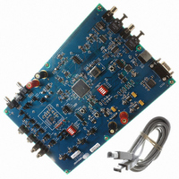
Manufacturer Part Number
CDB42L51
Description
BOARD EVAL FOR CS42L51 CODEC
Manufacturer
Cirrus Logic Inc
Specifications of CDB42L51
Main Purpose
Audio, CODEC
Embedded
Yes, Other
Utilized Ic / Part
CS42L51, CS8406, CS8415
Primary Attributes
Stereo, Digital Audio Transmitter and Receiver
Secondary Attributes
Graphic User Interface, S/PDIF Interface
Description/function
Audio CODECs
Operating Supply Voltage
5 V
Product
Audio Modules
For Use With/related Products
CS42L51
Lead Free Status / RoHS Status
Contains lead / RoHS non-compliant
Lead Free Status / RoHS Status
Lead free / RoHS Compliant, Contains lead / RoHS non-compliant
Other names
598-1005


DS679F1
HEADPHONE OUTPUT POWER CHARACTERISTICS
Test conditions (unless otherwise specified): Input test signal is a full-scale 997 Hz sine wave; measurement band-
width is 10 Hz to 20 kHz; Sample Frequency = 48 kHz; test load R
Parameter
AOUTx Power Into R
HP_GAIN[2:0]
000
001
010
011 (default)
100
101
110
111
8. One-half LSB of triangular PDF dither is added to data.
9. Full-scale output voltage and power is determined by the gain setting, G, in register
10. See
11. VA_HP settings lower than VA reduces the headroom of the headphone amplifier. As a result, the DAC
Gain (HP_GAIN[2:0])” on page
cause clipping when the audio signal approaches full-scale, maximum power output, as shown in
Figures 27
quired for the internal op-amp's stability and signal integrity. In this circuit topology, C
move the band-limiting pole of the amp in the output stage. Increasing this value beyond the recom-
mended 150 pF can cause the internal op-amp to become unstable.
may not achieve the full THD+N performance at full-scale output voltage and power.
Figure
Analog
Gain (G)
0.3959
0.4571
0.5111
0.6047
0.7099
0.8399
1.0000
1.1430
L
-
3. R
= 16
30 on page
L
Ω
and C
VA_HP
1.8 V
2.5 V
1.8 V
2.5 V
1.8 V
2.5 V
1.8 V
2.5 V
1.8 V
2.5 V
1.8 V
2.5 V
1.8 V
2.5 V
1.8 V
2.5 V
L
76.
reflect the recommended minimum resistance and maximum capacitance re-
Figure 3. Headphone Output Test Load
AGND
AOUTx
57. High gain settings at certain VA and VA_HP supply levels may
Min
-
-
-
-
-
-
-
-
VA = 2.5V (nominal)
0.022 µF
51 Ω
(Note 11)
(Note 11)
Typ
14
14
19
19
23
23
32
44
C
L
Max
L
= 16 Ω, C
-
-
-
-
-
-
-
-
(Note 9, 11)
R
L
Min
L
-
-
-
-
-
-
-
-
-
-
-
= 10 pF (see
VA = 1.8V (nominal)
(Note 9)
Typ
10
10
12
12
17
17
23
23
32
7
7
Figure
“Headphone Analog
Max
L
3).
-
-
-
-
-
-
-
-
-
-
-
will effectively
CS42L51
mW
mW
mW
mW
mW
mW
mW
mW
mW
mW
mW
mW
mW
mW
mW
mW
Unit
rms
rms
rms
rms
rms
rms
rms
rms
rms
rms
rms
rms
rms
rms
rms
rms
19
Related parts for CDB42L51
Image
Part Number
Description
Manufacturer
Datasheet
Request
R

Part Number:
Description:
Development Kit
Manufacturer:
Cirrus Logic Inc
Datasheet:
Part Number:
Description:
Development Kit
Manufacturer:
Cirrus Logic Inc
Datasheet:


Part Number:
Description:
High-efficiency PFC + Fluorescent Lamp Driver Reference Design
Manufacturer:
Cirrus Logic Inc
Datasheet:
Part Number:
Description:
Development Kit
Manufacturer:
Cirrus Logic Inc
Datasheet:
Part Number:
Description:
Development Kit
Manufacturer:
Cirrus Logic Inc
Datasheet:

Part Number:
Description:
Development Kit
Manufacturer:
Cirrus Logic Inc
Datasheet:
Part Number:
Description:
Development Kit
Manufacturer:
Cirrus Logic Inc
Datasheet:
Part Number:
Description:
Development Kit
Manufacturer:
Cirrus Logic Inc
Datasheet:
Part Number:
Description:
Development Kit
Manufacturer:
Cirrus Logic Inc
Datasheet:

Part Number:
Description:
EVALUATION BOARD FOR CS8427
Manufacturer:
Cirrus Logic Inc
Datasheet:

Part Number:
Description:
BOARD EVAL FOR CS8416 RCVR
Manufacturer:
Cirrus Logic Inc
Datasheet:

Part Number:
Description:
EVALUATION BOARD FOR CS8420
Manufacturer:
Cirrus Logic Inc
Datasheet:

Part Number:
Description:
KIT DEVELOPMENT EP9315 ARM9
Manufacturer:
Cirrus Logic Inc
Datasheet:

Part Number:
Description:
KIT DEVELOPMENT EP9302 ARM9
Manufacturer:
Cirrus Logic Inc
Datasheet: